On-chip mode multiplexing/demultiplexing method based on subwavelength grating structure

A subwavelength grating and mode multiplexing technology, applied in the field of optical communication, can solve the problems of large device size, difficult application, low tolerance of manufacturing process, etc., to achieve high tolerance and achieve the effect of high-order mode multiplexing

Inactive Publication Date: 2019-10-11
SHANGHAI JIAO TONG UNIV
View PDF2 Cites 5 Cited by
  • Summary
  • Abstract
  • Description
  • Claims
  • Application Information

AI Technical Summary

Problems solved by technology

Existing mode multiplexers/demultiplexers often have complex structures, large losses, la

Method used


Image

  • On-chip mode multiplexing/demultiplexing method based on subwavelength grating structure
  • On-chip mode multiplexing/demultiplexing method based on subwavelength grating structure
  • On-chip mode multiplexing/demultiplexing method based on subwavelength grating structure

Examples


Example Embodiment

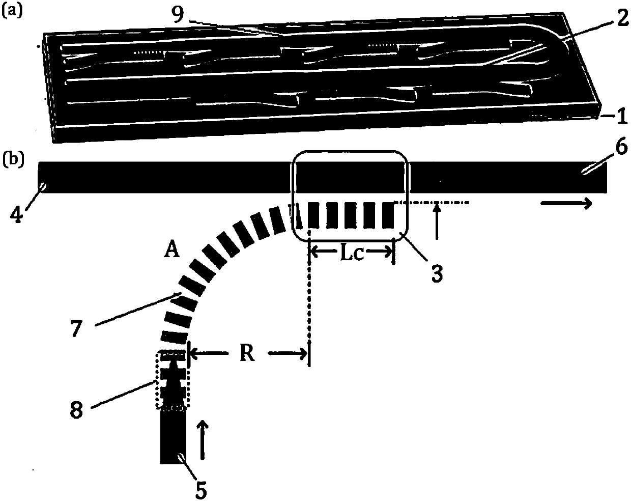
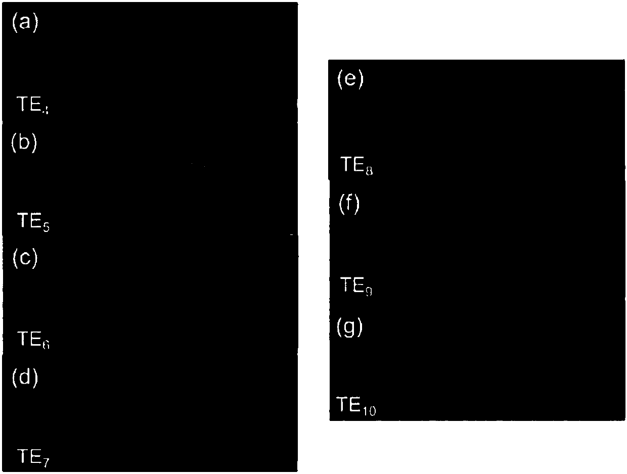
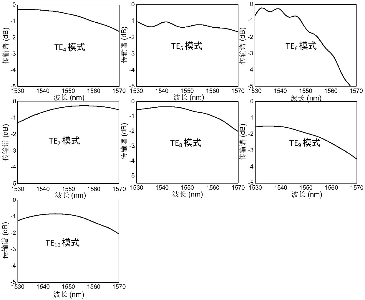
[0016] like figure 1 As shown, the present embodiment obtains seven cascaded directional couplers 3 processed on a silicon (SOI) platform on an insulating substrate 1, and injects TE from the input port 4 of the bus waveguide 0 In the transmission process, the fundamental mode is selectively input from the subwavelength grating input port 5, and then coupled to the bus waveguide 2 through the subwavelength grating cone 8, subwavelength grating waveguide 7 and strip waveguide 6 to become the corresponding high-order mode, the multi-channel signal continues to propagate forward in the bus waveguide, thereby realizing the multiplexing / demultiplexing of seven modes.

[0017] The processing refers to: realize on the SOI substrate by electron beam exposure and inductively coupled plasma etching, and then use plasma enhanced chemical vapor deposition to deposit 1 μm thick SiO 2 Thin films are deposited on the chip.

[0018] In this embodiment, each directional coupler 1 includes: a...


PUM

PropertyMeasurementUnit
Widthaaaaaaaaaa

Abstract

The present invention discloses an on-chip mode multiplexing/demultiplexing method based on a subwavelength grating structure, the method comprises: processing and obtaining seven cascaded directionalcouplers through an SOI platform, wherein each directional coupler comprises a strip waveguide and a sub-wavelength grating-shape waveguide, connecting the strip waveguide through an adiabatic cone to form a bus waveguide, then selectively inputting a fundamental mode from the each sub-wavelength grating-shape waveguide while injecting a TE0 mode from an input port of the bus waveguide, and achieving a coupling condition in the directional coupler to become a corresponding high-order mode, so that multiple signals simultaneously exist in the bus waveguide to realize mode multiplexing or demultiplexing. The method applies the subwavelength grating structure to the directional coupler, not only realizes multiplexing of seven high-order modes from TE4 to TE10 and the like, but also greatly reduces the device size.

Description

technical field [0001] The invention relates to a technology in the field of optical communication, in particular to a high-order mode multiplexing / demultiplexing purpose of realizing low loss and low crosstalk through a directional coupler with a sub-wavelength grating structure. Background technique [0002] In the existing long-distance optical fiber communication system, the channel capacity increase of the single-mode optical fiber transmission system cannot meet people's demand for bandwidth gradually, so improving the existing optical fiber transmission capacity has become an important direction of current research. Mode-division multiplexing technology uses the limited stable mode in multimode fiber as an independent channel to transmit information, which can double the system capacity and spectral efficiency, and is one of the key technologies for building future optical networks. Existing mode multiplexers / demultiplexers often have complex structures, large losses,...

Claims


Application Information

Patent Timeline
IPC IPC(8): G02B6/293
CPCG02B6/29325G02B6/2938G02B6/29395
Inventor 何宇张瑞环张永商启航张红霞苏翼凯
Owner SHANGHAI JIAO TONG UNIV
Why Eureka
Try Eureka