A fault-tolerant architecture for tsv in 3D integrated circuits

An integrated circuit, three-dimensional technology, applied in the direction of circuit, CAD circuit design, electrical components, etc., can solve the problems of unable to transmit signals normally, 3D chips are prone to failure, poor cluster fault tolerance, etc., to improve redundancy rate, Avoid the effect of too large difference in length and high repair rate

Active Publication Date: 2020-11-03
ANHUI POLYTECHNIC UNIV
View PDF6 Cites 1 Cited by
  • Summary
  • Abstract
  • Description
  • Claims
  • Application Information

AI Technical Summary

Problems solved by technology

3D chips are prone to faults during the manufacturing process, resulting in the failure to transmit signals normally
In response to this problem, Tingting Hwang et al. proposed a ring redundancy architecture, such as figure 1 As shown, although the area overhead is small, the tolerance to cluster faults is relatively poor, and the fault tolerance rate to 2*2 four faults is only about 50%.

Method used


Image

  • A fault-tolerant architecture for tsv in 3D integrated circuits
  • A fault-tolerant architecture for tsv in 3D integrated circuits
  • A fault-tolerant architecture for tsv in 3D integrated circuits

Examples


Embodiment Construction

[0027] In order to make the object, technical solution and advantages of the present invention clearer, the present invention will be further described in detail below in conjunction with the accompanying drawings and embodiments. It should be understood that the specific embodiments described here are only used to explain the present invention, not to limit the present invention.

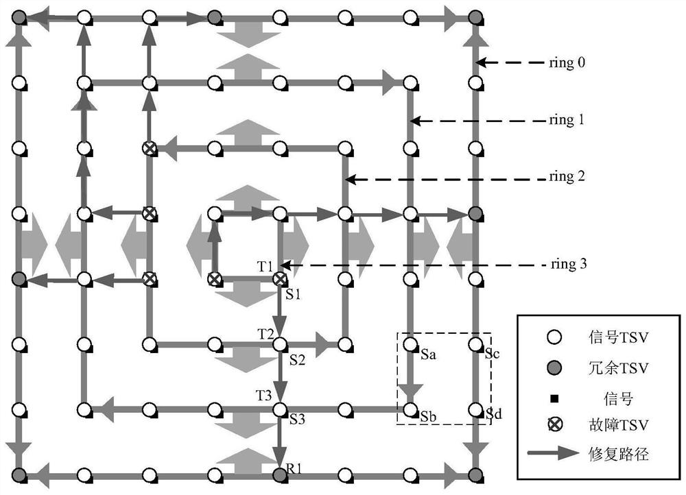
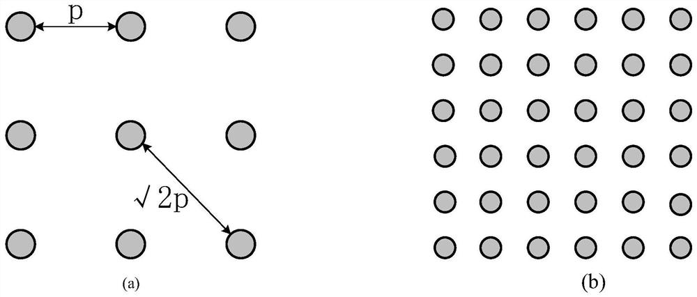
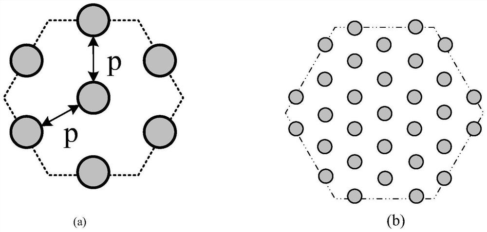
[0028] An important issue in the design process of a three-dimensional integrated circuit is the placement of TSVs, which are mainly responsible for signal transmission between layers. figure 2 (a) is a common 3×3 grid topology. There are 3 TSVs in each row and column of the TSV array, and a total of 9 TSVs are formed. figure 2 In (a), p is the pitch, that is, the distance between adjacent TSVs. In the grid topology, the TSV distance between the TSV and the adjacent horizontal and vertical direction is p, and the TSV distance from the center point TSV to the diagonal position is The distance b...


PUM


Abstract

The present invention is applicable to the field of semiconductor technology, and provides a fault-tolerant architecture for TSVs in three-dimensional integrated circuits. The redundant structure is composed of an N-layer ring structure, and the N-layer ring structure is divided into six regions by six rays, and each ring layer There are three RTSVs in the structure, and the three RTSVs are evenly distributed on the six rays. The RTSVs between adjacent layers are misplaced. The center of the innermost hexagon is equipped with an RTSV, which utilizes the unique symmetry and flexibility of the hexagon. Arrange TSVs in a consistent manner, and select and place RTSVs reasonably, divide the redundant structure into several uniform areas, improve the redundancy rate of each area, and ensure a high repair rate of the entire structure; the uniform distribution of RTSVs in the TSV array, combined with The symmetry of the routing direction can avoid the situation that the repair path length of the faulty TSV is too different or the timing overhead is large, and the overhead can be reduced.

Description

technical field [0001] The invention belongs to the technical field of semiconductors and provides a fault-tolerant architecture for TSVs in three-dimensional integrated circuits. Background technique [0002] As the semiconductor process continues to approach the scale of 5nm, 3nm, and 1nm, Moore's Law is also approaching the physical limit. Rico Wiedenbruch, senior vice president of Merck's Global Integrated Circuit Materials Division, said that changing the structure of semiconductor chips through 3D chip structures is the best way to solve the increasingly difficult problem of process size reduction when Moore's Law approaches the physical limit. answer. Three-dimensional integrated circuits (3D IC) use through-silicon vias (Though Silicon Via, TSV) to connect different layers of devices such as different chips or circuit modules in the vertical direction. Compared with two-dimensional integrated circuits, 3D ICs can effectively reduce the length of interconnection lin...

Claims


Application Information

Patent Timeline
Patent Type & Authority Patents(China)
IPC IPC(8): H01L27/02H01L23/48G06F30/398G06F115/06
CPCH01L27/0207H01L23/481G06F30/398G06F2115/06
Inventor 倪天明束月鲁麟代广珍韩名君高文根瞿成明朱世东
Owner ANHUI POLYTECHNIC UNIV
Why Eureka
Try Eureka