Micro LED mass transfer device and method based on demagnetization through selective heating

A transfer device and transfer method technology, applied in the field of mass transfer, can solve the problems of uneven stretching time interval, high cost of patterning laser, troublesome stamp making, etc. Effect

Active Publication Date: 2019-10-15
HUAZHONG UNIV OF SCI & TECH
View PDF8 Cites 19 Cited by
  • Summary
  • Abstract
  • Description
  • Claims
  • Application Information

AI Technical Summary

Problems solved by technology

At present, the selective transfer technologies are as follows: 1) Variable pitch transfer by film stretching and patterning laser, which is achieved by temporarily bonding chips on the polymer transparent film stretching layer, and then stretching the transparent film Realize the adjustment of the chip spacing, and finally release the chip with a patterned laser. This method has problems such as uneven stretching time, and the cost of the patterned laser is high; 2) Selective transfer is achieved by transfer stamps. Transfer stamps with microstructures are patterned, selectively pick up chips, and then release the chips on the circuit substrate. This method is more troublesome to make stamps, and there are problems such as inaccurate positioning.

Method used


Image

  • Micro LED mass transfer device and method based on demagnetization through selective heating
  • Micro LED mass transfer device and method based on demagnetization through selective heating
  • Micro LED mass transfer device and method based on demagnetization through selective heating

Examples


Embodiment Construction

[0032] In order to make the object, technical solution and advantages of the present invention clearer, the present invention will be further described in detail below in conjunction with the accompanying drawings and embodiments. It should be understood that the specific embodiments described here are only used to explain the present invention, not to limit the present invention. In addition, the technical features involved in the various embodiments of the present invention described below can be combined with each other as long as they do not constitute a conflict with each other.

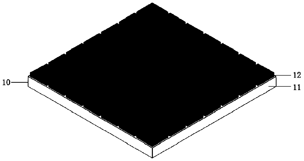
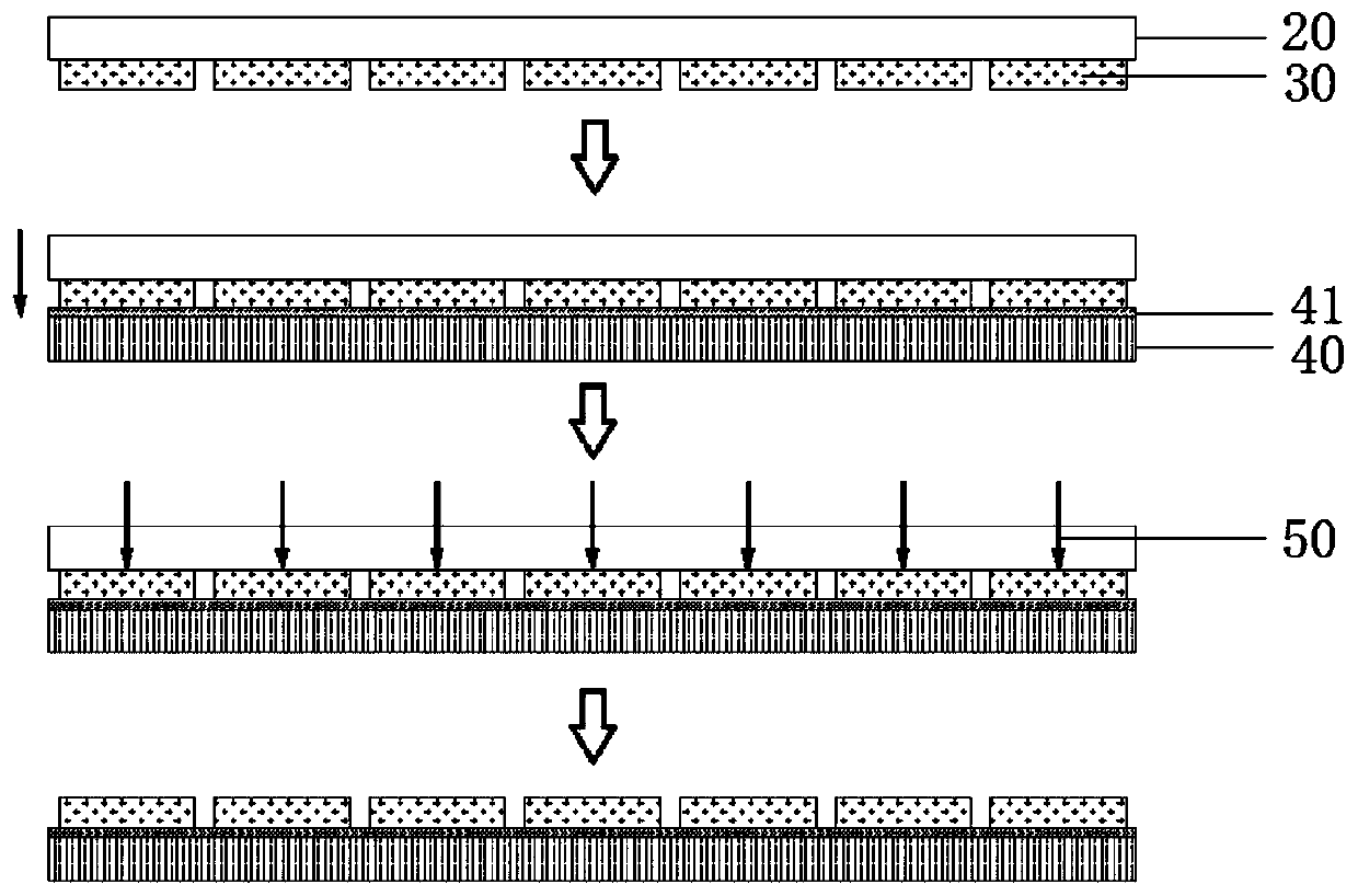
[0033] Such as Figure 1-2As shown, the embodiment of the present invention provides a micro light-emitting diode (MicroLED) mass transfer device based on selective heating and demagnetization. The device includes a substrate 11 and a magnetic square array 12 arranged on the upper surface of the substrate 11. The magnetic squares Each magnetic square in the array 12 is magnetic, and the upper a...


PUM

PropertyMeasurementUnit
sizeaaaaaaaaaa
Curie pointaaaaaaaaaa

Abstract

The invention belongs to the technical field of mass transfer, and particularly discloses a Micro LED mass transfer device and method based on demagnetization through selective heating. The device comprises a substrate and a magnetic square array arranged on the upper surface of the substrate, wherein each magnetic square in the magnetic square array has magnetism, and the upper surface and the lower surface of each magnetic square are different magnetic poles; each magnetic square can lose magnetism under the action of external heating. When transfer operation is performed, the magnetic square array is in one-to-one correspondence with the Micro LED array with the magnetism, the magnetic square array is adopted to integrally pick up the Micro LED array, then the magnetic squares are selectively heated to allow the magnetic squares to lose the magnetism to selectively transfer the Micro LED onto a target circuit substrate with the magnetism. The Micro LED mass transfer device and method can achieve the patterning and selectivity mass transfer of the Micro LED, and is high in applicability and accurate in positioning, etc.

Description

technical field [0001] The invention belongs to the technical field of mass transfer, and more specifically relates to a Micro LED mass transfer device and method based on selective heating and demagnetization. Background technique [0002] Micro LED (μLED) is a new generation of display technology, which has higher brightness, higher luminous efficiency, longer life and lower power consumption than the existing organic light emitting diode (OLED). Micro light-emitting diodes have the characteristics of self-illumination and no need for a backlight source, and each pixel can be addressed and turned on individually. [0003] The manufacturing process of micro-light-emitting diode displays is usually to thin, miniaturize, and array the diode (LED) structure so that its size is only about 10 microns, and then transfer a large number (tens of thousands to tens of millions) of micro-light-emitting diode chips Form an LED array on the display circuit substrate, and finally packag...

Claims


Application Information

Patent Timeline
Patent Type & Authority Applications(China)
IPC IPC(8): H01L21/683H01L21/67H01L33/48H01L25/075H01F13/00
CPCH01F13/006H01L21/67271H01L21/6835H01L21/6836H01L25/0753H01L33/48H01L2221/68368H01L2221/68381H01L2933/0033
Inventor 黄永安杨彪卞敬尹周平陈建魁
Owner HUAZHONG UNIV OF SCI & TECH
Why Eureka
Try Eureka