Phase change memory and manufacturing method thereof

A technology of phase change memory and manufacturing method, which is applied in the field of phase change memory and its manufacture, and can solve the problems that phase change memory cannot meet the application requirements of storage type memory, etc.

Inactive Publication Date: 2019-10-15
SHANGHAI INST OF MICROSYSTEM & INFORMATION TECH CHINESE ACAD OF SCI
View PDF9 Cites 13 Cited by
  • Summary
  • Abstract
  • Description
  • Claims
  • Application Information

AI Technical Summary

Problems solved by technology

[0005] In view of the shortcomings of the prior art described above, the purpose of the present invention is to provide a method for manufacturing a phase-change memory, which is used to solve the problem that the phase-change memory in the prior art cannot meet the application requirements of storage-type memory

Method used


Image

  • Phase change memory and manufacturing method thereof
  • Phase change memory and manufacturing method thereof
  • Phase change memory and manufacturing method thereof

Examples


Embodiment 1

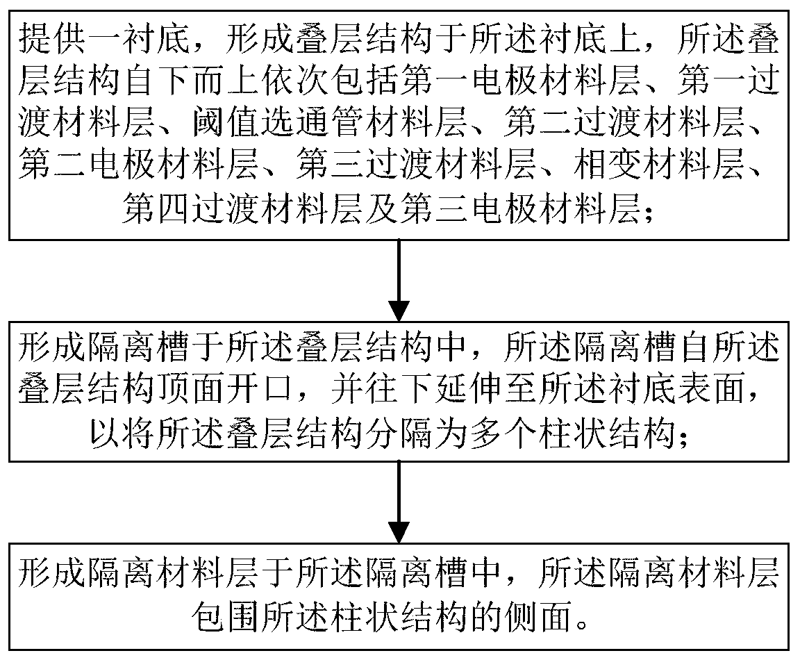
[0056] The present invention provides a manufacturing method of phase change memory, please refer to figure 1 , shown as a process flow diagram of the method, comprising the following steps:

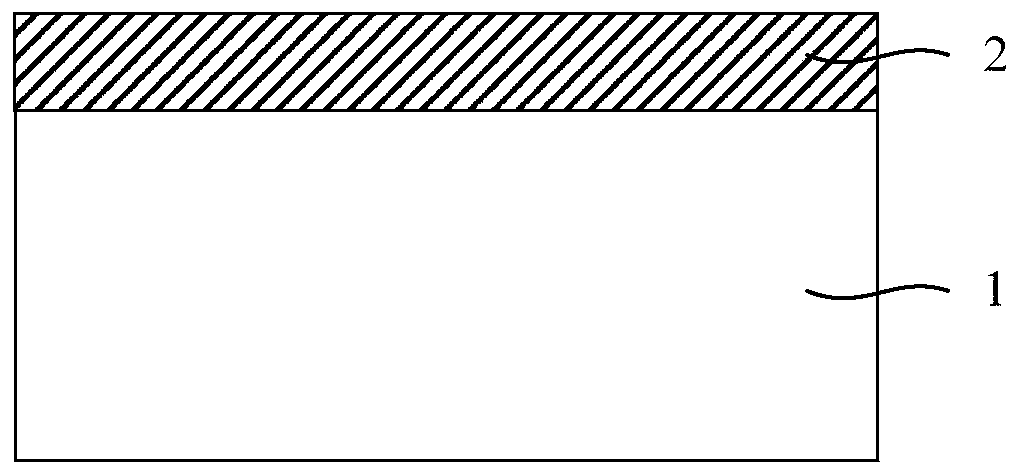
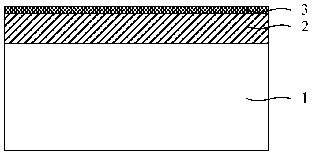
[0057] S1: Provide a substrate, and form a laminated structure on the substrate, the laminated structure sequentially includes a first electrode material layer, a first transition material layer, a threshold gate material layer, a second transition material layer, second electrode material layer, third transition material layer, phase change material layer, fourth transition material layer and third electrode material layer;

[0058] S2: forming isolation grooves in the stacked structure, the isolation grooves are opened from the top surface of the stacked structure, and extend down to the surface of the substrate, so as to separate the stacked structure into a plurality of columns structure;

[0059] S3: Form an isolation material layer in the isolation groove, the isolation material ...

Embodiment 2

[0091] The present invention also provides a phase change memory, please refer to Figure 12 , showing a schematic cross-sectional structure of the phase-change memory, including a substrate 1, an isolation material layer 12 and a plurality of phase-change memory cells, wherein the plurality of phase-change memory cells are separately arranged on the substrate 1, so The phase-change memory cell has a columnar structure, which includes a first electrode material layer 2, a first transition material layer 3, a threshold gate material layer 4, a second transition material layer 5, and a second electrode material layer 6 from bottom to top. , a third transition material layer 7, a phase change material layer 8, a fourth transition material layer 9 and a third electrode material layer 10; the isolation material layer 12 is located on the substrate 1 and surrounds the phase change memory unit Each of the phase change memory cells is isolated from each other by the isolation material...


PUM


Abstract

The invention provides a phase change memory and a manufacturing method thereof. The phase change memory comprises a substrate, a plurality of phase change memory units and isolation material layers.The phase change memory units are discretely arranged on the substrate. Each phase change memory unit comprises a first electrode material layer, a first transition material layer, a threshold gate tube material layer, a second transition material layer, a second electrode material layer, a third transition material layer, a phase change material layer, a fourth transition material layer and a third electrode material layer in turn from bottom to top. The isolation material layers are located on the substrate and surround the sides of the phase change memory units, and the phase change memoryunits are isolated from one another through the isolation material layers. In the phase change memory of the invention, the phase change material and the OTS material are limited in the same space bythe isolation material, and the transition material layers are located between the phase change material and the electrode material, between the phase change material and the OTS material and betweenthe OTS material and the electrode material, so that the phase change memory has the characteristics of high density, high speed, low power consumption and long life.

Description

technical field [0001] The invention belongs to the technical field of microelectronics, and relates to a phase-change memory and a manufacturing method thereof. Background technique [0002] In the traditional computing architecture, the significant performance difference between DRAM and NAND Flash makes the response efficiency of the north-south bridge data exchange in large data centers and computers and other equipment low and the energy consumption remains high. In recent years, the industrial and scientific circles have invested a lot of manpower, material resources, and financial resources in the research of new storage technologies. Large enterprises represented by IBM, Intel, Micron, and Samsung are all seeking new high-performance storage technologies, which are called storage memory. (SCM-Storage Class Memory), fill the performance gap between DRAM and Flash, or partially replace DRAM and Flash, to build a new storage architecture to improve overall performance. ...

Claims


Application Information

Patent Timeline
Patent Type & Authority Applications(China)
IPC IPC(8): H01L45/00H01L27/24
CPCH10B63/80H10N70/231H10N70/8616H10N70/011H10B63/24H10N70/841H10N70/882H10N70/8825H10N70/826H10N70/8828H10N70/063
Inventor 宋志棠宋三年
Owner SHANGHAI INST OF MICROSYSTEM & INFORMATION TECH CHINESE ACAD OF SCI
Why Eureka
Try Eureka