A kind of semiconductor structure and its manufacturing method

A manufacturing method and semiconductor technology, which is applied in semiconductor/solid-state device manufacturing, electrical components, circuits, etc., can solve problems such as being easily affected by film thickness, unfavorable control of the processing window of key dimensions of the bottom, and achieve the effect of increasing the processing window

Active Publication Date: 2020-05-19
YANGTZE MEMORY TECH CO LTD
View PDF5 Cites 0 Cited by
  • Summary
  • Abstract
  • Description
  • Claims
  • Application Information

AI Technical Summary

Problems solved by technology

[0004] In view of the above-mentioned shortcomings of the prior art, the purpose of the present invention is to provide a semiconductor structure and its manufacturing method, which is used to solve the problem that the critical dimension of the bottom of the hole in the prior art is easily affected by the film thickness, which is not conducive to the processing window of the critical dimension of the bottom. the problem of control

Method used


Image

  • A kind of semiconductor structure and its manufacturing method
  • A kind of semiconductor structure and its manufacturing method
  • A kind of semiconductor structure and its manufacturing method

Examples


Embodiment 1

[0096] In this embodiment, a manufacturing method of a semiconductor structure is provided, please refer to Picture 9 , Shown as the process flow chart of the method, including the following steps:

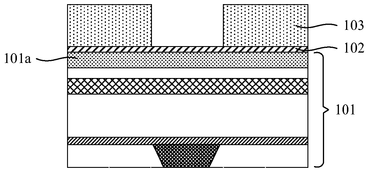
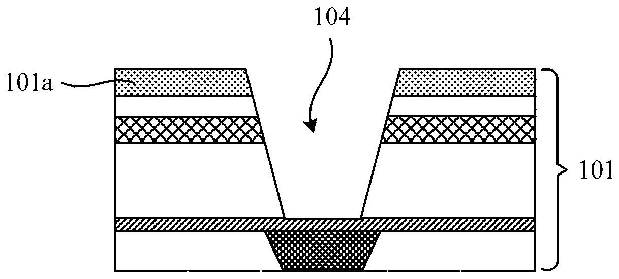
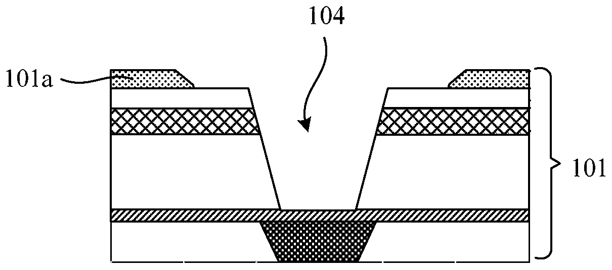
[0097] See Picture 10 , A layer stack structure 301 is provided, the layer stack structure includes an insulating dielectric interlayer 301a, an etching stop layer 301b located below the insulating dielectric interlayer 301a, and a first hard mask layer 301c located above the insulating dielectric interlayer 301a And a second hard mask layer 301d located above the first hard mask layer 301c. In this embodiment, an insulating layer 301e is further provided between the first hard mask layer 301c and the second hard mask layer 301d, and the material of the insulating layer 301e includes but is not limited to silicon dioxide. The layer stack structure 301 is further provided with a contact portion 301f, and the contact portion 301f is located under the etching stop layer 301b.

[0098] ...

Embodiment 2

[0115] The invention in this embodiment also provides a semiconductor structure, please refer to Figure 17 , Shown as a schematic diagram of the semiconductor structure, including a layer stack structure 401, a first recessed structure and a second recessed structure, wherein the layer stack structure 401 includes an insulating dielectric interlayer 401a, an etching located under the insulating dielectric interlayer 401a The barrier layer 401b, the hard mask layer 401c located above the insulating dielectric interlayer 401a, and the insulating layer 401d located above the hard mask layer 401c, the first recess structure 402 opens from the top surface of the insulating layer 401d, And extends downward into the insulating dielectric interlayer 401a, but does not penetrate the insulating dielectric interlayer 401a. The second recessed structure 403 opens from the bottom surface of the first recessed structure 402 and extends downwards through the etching For the barrier layer 401b...


PUM

PropertyMeasurementUnit
angleaaaaaaaaaa

Abstract

The invention provides a semiconductor structure and a manufacturing method thereof, and the method comprises the following steps: providing a stacked structure, and forming a first recessed structurein the stacked structure, wherein the first recessed structure extends downwards into an insulating medium interlayer but does not penetrate through an insulating medium interlayer; etching the insulating medium interlayer by taking a first hard mask layer as a mask to obtain a second concave structure in the stacked structure, wherein the second concave structure extends to the surface of the etching barrier layer and has a vertical side wall; transversely trimming the second hard mask layer to enlarge the size of a top opening of the second hard mask layer; and etching the insulating mediuminterlayer by taking the second hard mask layer as a mask so as to enlarge the opening size of the first concave structure in the insulating medium interlayer. The method can adapt to dual damascenehole patterns, slit patterns or groove pattern structures with different film thicknesses, and is beneficial to enlarging a processing window of chemical mechanical polishing of an insulating layer ina preorder process and enlarging a processing window of a key size at the bottom of a dual damascene hole.

Description

Technical field [0001] The invention belongs to the field of semiconductor integrated circuits, and relates to a semiconductor structure and a manufacturing method thereof. Background technique [0002] At present, the merging of hole-shaped grooves and T-shaped holes can be achieved by using only one development and etching process to achieve a double damascene hole type (or slit type (slit), trench type (trench)) structure, that is, in the smaller After the CD mask is developed, a part of the hole is etched and then the mask is enlarged by a horizontal trimming (Trim) method, and then the remaining holes are further etched. When the post-etching inspection (AEI) is fixed and the initial top critical dimension is greater than the bottom critical dimension, when the OX film thickness variation is large, the bottom critical dimension will change with the film thickness. Thicker or thinner and correspondingly smaller or larger, which is not conducive to the control of the processi...

Claims


Application Information

Patent Timeline
Patent Type & Authority Patents(China)
IPC IPC(8): H01L21/762
CPCH01L21/76205H01L21/7621
Inventor 杨罡
Owner YANGTZE MEMORY TECH CO LTD
Why Eureka
Try Eureka