
Method for forming dopant well and method for forming image sensor

An image sensor and deep doping technology, applied in semiconductor/solid-state device manufacturing, electrical components, circuits, etc., can solve the problem of difficulty in controlling the increase of key dimensions, and achieve the effect of uniform key dimensions and simplified process steps

Inactive Publication Date: 2010-12-22
SEMICONDUCTOR MANUFACTURING INTERNATIONAL (BEIJING) CORP
View PDF1 Cites 0 Cited by
  • Summary
  • Abstract
  • Description
  • Claims
  • Application Information

AI Technical Summary

Problems solved by technology

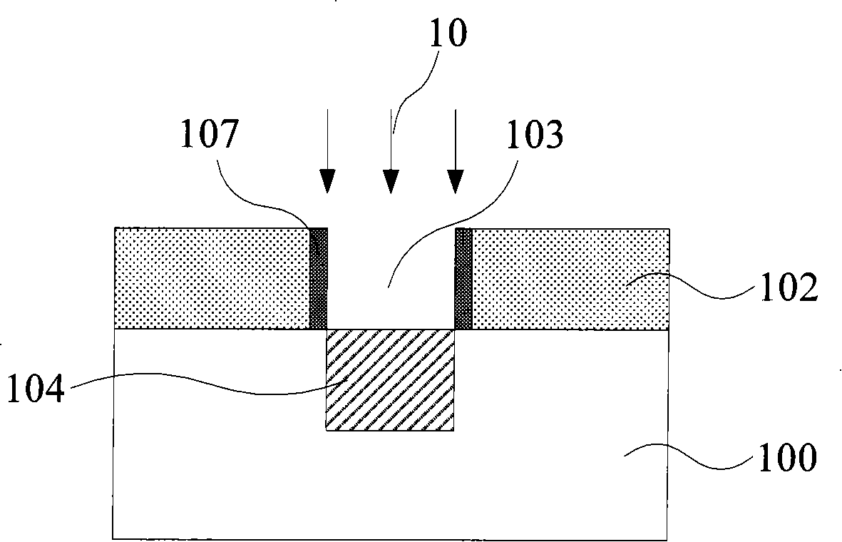
[0008] In the prior art, when the first ion implantation is performed on the semiconductor substrate, the ions will react with the sidewall of the photoresist layer of the opening pattern of the first ion implantation to form a hardened substance different in nature from the photoresist layer, When the photoresist layer is subsequently ashed with oxygen to increase the critical dimension of the opening pattern of the first ion implantation, the increase of the critical dimension is difficult to control

Method used


Image

  • Method for forming dopant well and method for forming image sensor
  • Method for forming dopant well and method for forming image sensor
  • Method for forming dopant well and method for forming image sensor

Examples


Embodiment Construction

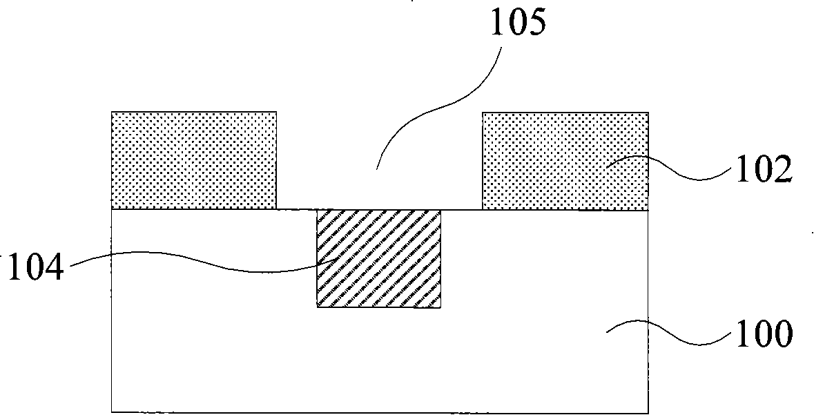
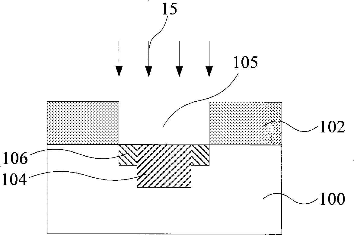
[0025] The invention etches the photoresist layer and the silicon oxide layer to expose the semiconductor substrate to define the doped well pattern; ash the photoresist layer to expose the silicon oxide layer to increase the critical dimension of the doped well pattern; The key dimensions of the doped well pattern are defined in advance, so they will not be affected by the implanted ions, and the key dimensions can be controlled uniformly. Furthermore, because only one ion implantation is required, a doped well with depth gradient distribution can be obtained, and the process steps are simplified.

[0026] In order to make the above objects, features and advantages of the present invention more comprehensible, specific implementations of the present invention will be described in detail below in conjunction with the accompanying drawings.

[0027] Figure 4 It is a flow chart of a specific embodiment of forming a depth gradient distribution doped well in the present inventio...


PUM


Abstract

The invention relates to a method for forming a dopant well and a method for forming an image sensor. The method for forming the dopant well comprises the following steps: forming a silicon oxide layer on a semiconductor substrate; etching a photoresist layer and a silicon oxide layer until the layers are exposed out of the semiconductor substrate after forming the photoresist layer on the siliconoxide layer, and defining the graphics of the dopant well; incinerating the photoresist layer until the layer is exposed out of the silicon oxide layer, and increasing the key dimension of the graphics of the dopant well; taking the photoresist layer and the silicon oxide layer as masks, implanting ions into the semiconductor substrate along the increased graphics of the dopant well, and formingthe dopant well of which the depth is in graded distribution; and removing the photoresist layer and the silicon oxide layer. The invention also provides the method for forming the image sensor. The invention can uniformly control the key dimension of the dopant well and simplifies processing steps.

Description

technical field [0001] The invention relates to the field of semiconductor technology, in particular to a method for forming a doped well and an image sensor. Background technique [0002] With the continuous development of semiconductor technology, the degree of integration of semiconductor devices is also getting higher and higher. Therefore, the requirements for critical dimensions of semiconductor devices are also getting higher and higher. [0003] While controlling the critical dimensions of semiconductor devices, in order to optimize the junction depth and reduce leakage, there are also requirements for the contact area between semiconductor devices. For example, in the existing process of making photodiode doped wells for image sensors, The doped well is made into an ion depth distribution gradient to increase the contact area with the semiconductor substrate, that is, the PN junction area, thereby increasing the junction capacitance, increasing the resistance, impro...

Claims


Application Information

Patent Timeline
Patent Type & Authority Patents(China)
IPC IPC(8): H01L21/822H01L27/146
Inventor 洪中山刘蓓霍介光
Owner SEMICONDUCTOR MANUFACTURING INTERNATIONAL (BEIJING) CORP
Learn More