
Method for forming gate structure of NAND memory, NAND memory and photomask

A gate structure and memory technology, applied in the field of NAND memory and photomask mask, can solve the problem of load effect weakening the influence of registration deviation between layers and so on

Inactive Publication Date: 2020-05-05
SHANGHAI HUALI MICROELECTRONICS CORP
View PDF3 Cites 0 Cited by
  • Summary
  • Abstract
  • Description
  • Claims
  • Application Information

AI Technical Summary

Problems solved by technology

[0006] The purpose of the present invention is to provide a method for forming a gate structure of NAND memory, to solve the problem of load effect during sidewall etching and to weaken the impact of interlayer registration deviation on subsequent processes

Method used


Image

  • Method for forming gate structure of NAND memory, NAND memory and photomask
  • Method for forming gate structure of NAND memory, NAND memory and photomask
  • Method for forming gate structure of NAND memory, NAND memory and photomask

Examples


Embodiment Construction

[0035] The technical solutions in the present invention will be clearly and completely described below in conjunction with the accompanying drawings. Apparently, the described embodiments are part of the embodiments of the present invention, not all of them. Based on the embodiments of the present invention, all other embodiments obtained by persons of ordinary skill in the art without making creative efforts belong to the protection scope of the present invention.

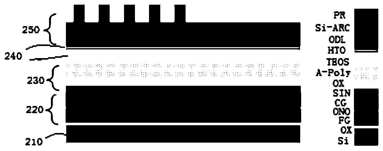
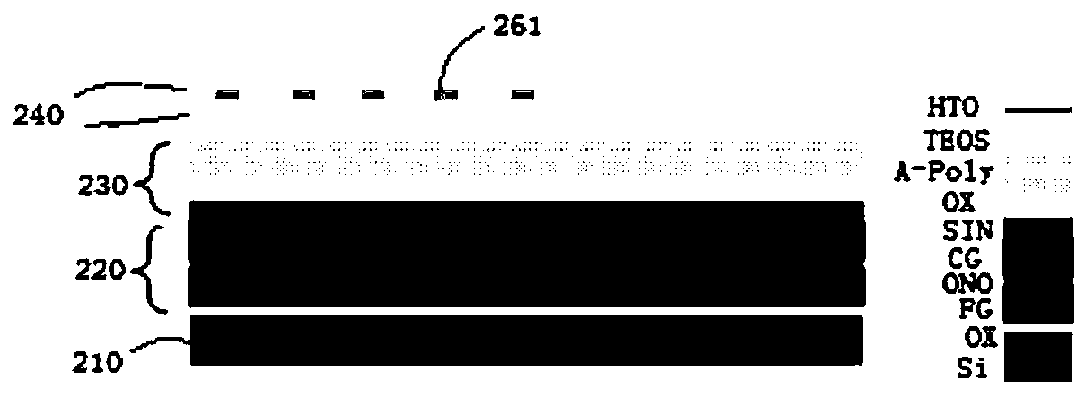
[0036] Specifically, see Figures 2a-2g , Figures 2a-2g It is a schematic diagram of the manufacturing process of the prior art NAND memory, such as Figures 2a-2g Shown, the manufacturing process of the NAND memory of prior art comprises:

[0037] S1: Provide a substrate 210, on which a gate structure layer 220, a pattern transfer layer 230, a mandrel pattern layer 240, and an organic dielectric Tri-Layer layer 250 are sequentially formed, such as Figure 2a shown;

[0038] S2: to Figure 3a The photomask s...


PUM


Abstract

The invention relates to a gate structure forming method of an NAND memory, a NAND memory and a photomask, and relates to a semiconductor integrated circuit manufacturing process. The method comprisesthe steps of in the forming process of the gate structure of the NAND memory, forming a mandrel pattern shape for forming a control gate structure through a first photoetching exposure process, and forming a mandrel pattern morphology used for forming a peripheral gate structure and a selection gate structure; then, in the process of removing the mandrel pattern structure through a second photoetching exposure process, protecting an area for forming the peripheral gate and selection gate structures by using photoresist so as to remove the control gate mandrel film layer; in the subsequent etching of the gate structure, forming the control gate by the remaining side walls; and forming the peripheral gate and the selection gate by the side walls and the unremoved mandrel pattern structure together. The critical size of the side wall used for forming the outermost periphery of the control gate is not large, and the influence of interlayer registration deviation on the subsequent processis weakened.

Description

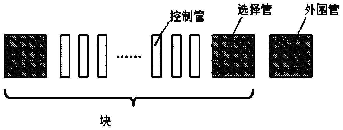
technical field [0001] The invention relates to a manufacturing process of a semiconductor integrated circuit, in particular to a gate structure forming method of a NAND memory, a NAND memory and a photomask mask. Background technique [0002] In semiconductor integrated circuits, NAND memory (NAND flash) is a non-volatile memory. Due to its large capacity, fast erasing and writing speed, and low cost, it is suitable for data storage and is widely used in consumer, automotive, and industrial electronics. and other fields. [0003] see figure 1 , figure 1 It is a schematic diagram of the architecture of NAND memory, such as figure 1 As shown, a NAND memory is usually composed of a storage area and a peripheral area. The peripheral area is composed of a plurality of peripheral tubes. The storage area is further composed of a plurality of blocks. Each block consists of two selector tubes and several control tubes. The selection tubes are located at both ends of the block...

Claims


Application Information

Patent Timeline
Patent Type & Authority Applications(China)
IPC IPC(8): H01L21/28H01L29/423H01L27/11524H01L27/11521H01L27/1157H01L27/11568H10B41/30H10B41/35H10B41/41H10B41/46H10B41/47H10B43/30H10B43/35
CPCH01L21/28008H01L29/42356H10B41/30H10B41/35H10B43/30H10B43/35H01L29/40114H01L29/66825H01L29/788H10B41/41H10B41/46H10B41/47H01L29/42328
Inventor 许鹏凯乔夫龙王一
Owner SHANGHAI HUALI MICROELECTRONICS CORP
Learn More