Semiconductor storage device and preparation method thereof

A storage device and semiconductor technology, which is applied in the fields of semiconductor/solid-state device manufacturing, semiconductor devices, and semiconductor/solid-state device components, etc., can solve problems such as the inability to meet the resolution requirements of manufacturing micro-line width patterns or manufacturing process requirements, and achieves a reduction in size. The effect of small impedance and reduced preparation difficulty

Pending Publication Date: 2022-02-18
FUJIAN JINHUA INTEGRATED CIRCUIT CO LTD
View PDF0 Cites 0 Cited by
  • Summary
  • Abstract
  • Description
  • Claims
  • Application Information

AI Technical Summary

Problems solved by technology

[0003] With the complexity of integrated circuits, the size of these tiny patterns is continuously reduced and the structure is constantly changing. Therefore, the equipment used to generate feature patterns must meet the strict requirements of manufacturing process resolution and overlay accuracy. , the single patterning method can no longer meet the resolution requirements or manufacturing process requirements for manufacturing micro-linewidth patterns

Method used


Image

  • Semiconductor storage device and preparation method thereof
  • Semiconductor storage device and preparation method thereof
  • Semiconductor storage device and preparation method thereof

Examples


Embodiment Construction

[0039] The semiconductor storage device and its manufacturing method will be further described below with reference to the accompanying drawings and embodiments.

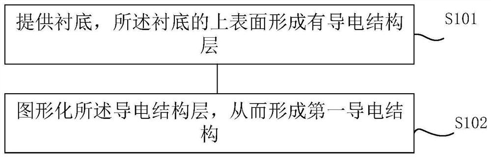
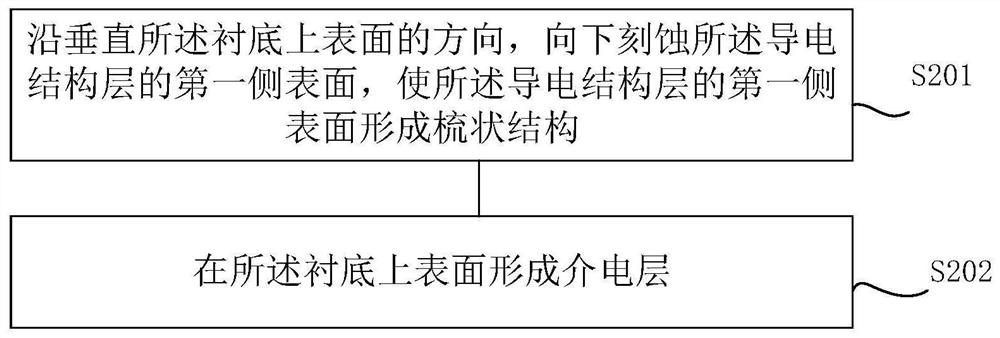
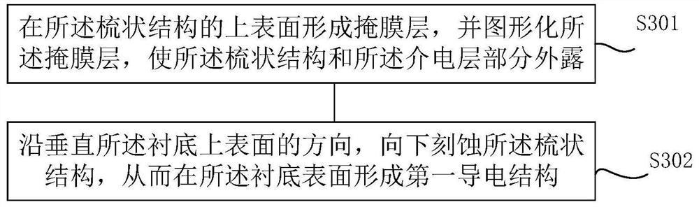
[0040] see figure 1 , is a schematic diagram of the steps of the method for manufacturing a semiconductor storage device in an embodiment of the present application.

[0041] In this embodiment, a method for manufacturing a semiconductor storage device provided by the present application includes the following steps:

[0042] Step S101 : providing a substrate 101 with a conductive structure layer formed on the upper surface of the substrate 101 . here as Figure 6 as shown, Figure 6 It is a schematic side view of the semiconductor storage device when the semiconductor storage device is prepared in an embodiment of the present application.

[0043] The substrate 101 includes a semiconductor base and several film layers formed on the surface of the semiconductor base.

[0044] The material of the semiconductor s...


PUM


Abstract

The invention discloses a semiconductor storage device and a preparation method thereof, which can meet the resolution requirement or the manufacturing process requirement for manufacturing micro line width patterns. The preparation method of the semiconductor storage device comprises the following steps of providing a substrate, wherein a conductive structure layer is formed on an upper surface; patterning the conductive structure layer to form a first conductive structure comprising a first pattern structure, the first pattern structure extending in a first direction and having a first width in a second direction perpendicular to the first direction, the first pattern structure further comprising a terminal conductive structure having a second width in a second direction perpendicular to the first direction, the terminal conductive structure comprising an inner side widening part and an outer side widening part which are sequentially arranged along the first direction, the inner side widening part and the outer side widening part being respectively used for extending the first pattern structure along the third direction and extending the first pattern structure along the fourth direction, and the third direction and the fourth direction being not parallel to the first direction.

Description

technical field [0001] The present application relates to the field of semiconductor devices, in particular to a semiconductor storage device and a manufacturing method thereof. Background technique [0002] In the semiconductor manufacturing process, the manufacture of some microstructures requires the use of photolithography and etching in appropriate substrates or material layers such as semiconductor substrates / film layers, dielectric material layers, or metal material layers to form microstructures with Tiny patterns of precise dimensions. For this purpose, in conventional semiconductor technology, a mask layer (masklayer) is formed on the target material layer, so that these tiny patterns are first formed / defined in the mask layer, and then the patterns are transferred to target layer. Generally speaking, the mask layer is, for example, a patterned photoresist layer formed by a photolithography process, and / or a patterned mask layer formed using the patterned photore...

Claims


Application Information

Patent Timeline
Patent Type & Authority Applications(China)
IPC IPC(8): H01L21/768H01L23/48
CPCH01L21/7688H01L21/7681H01L23/481
Inventor 陈云詹益旺陈凡刘强李宝玉江丽贞
Owner FUJIAN JINHUA INTEGRATED CIRCUIT CO LTD
Why Eureka
Try Eureka