A kind of formation method of high-k metal gate

A metal gate and formation layer technology, which is applied to semiconductor devices, electrical components, circuits, etc., can solve the problems of device reliability impact, increased risk of metal voids, and increased surface roughness of trenches, so as to increase critical dimensions, eliminate The effect of metal voids

Active Publication Date: 2019-03-26
SHANGHAI HUALI MICROELECTRONICS CORP
View PDF4 Cites 0 Cited by
  • Summary
  • Abstract
  • Description
  • Claims
  • Application Information

AI Technical Summary

Problems solved by technology

In the process of removing the dummy gate oxide, the surface roughness of the channel will become larger. At the same time, during the etching process, whether it is dry etching or wet etching, harmful substances such as F ions will be introduced. Impurity ions
These ions diffuse into the channel and have a severe impact on the reliability of the device
At the same time, a high-K film will be deposited on the sidewall, and the gap that can be filled by the gate will be reduced by almost 4nm, which greatly increases the risk of metal voids.

Method used


Image

  • A kind of formation method of high-k metal gate
  • A kind of formation method of high-k metal gate
  • A kind of formation method of high-k metal gate

Examples


Embodiment Construction

[0019] In order to make the content of the present invention clearer and easier to understand, the content of the present invention will be described in detail below in conjunction with specific embodiments and accompanying drawings.

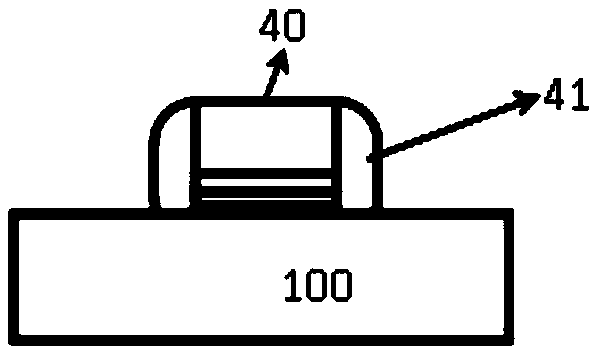
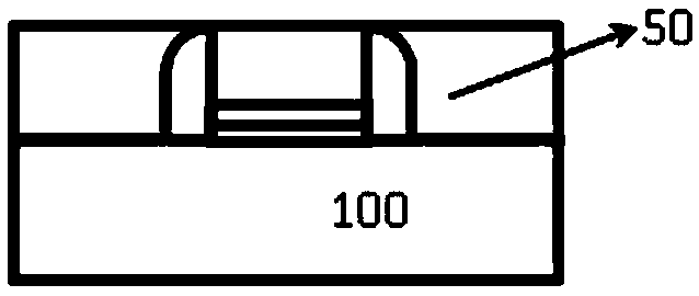
[0020] Figure 1 to Figure 6 Each step of the method for forming a high-K metal gate according to a preferred embodiment of the present invention is schematically shown.

[0021] Specifically, such as Figure 1 to Figure 6 As shown, the method for forming a high-K metal gate according to a preferred embodiment of the present invention includes:

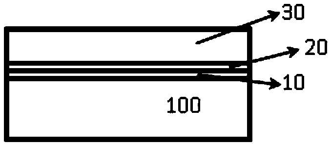
[0022] The first step: sequentially forming an interlayer dielectric layer 10, a TiO2 thin film layer 20 and a polysilicon layer 30 on a substrate 100;

[0023] Preferably, the interlayer dielectric layer 10 is a SiO2 film layer. Preferably, the growth method of the interlayer dielectric layer 10 may be chemical vapor deposition, atomic layer deposition, thermal oxidation, low-pressure chemical vapor...


PUM

PropertyMeasurementUnit
thicknessaaaaaaaaaa
thicknessaaaaaaaaaa

Abstract

The invention provides a forming method of a high-K metal grid. The method comprises the following steps of step 1: sequentially forming an interlayer dielectric layer, a TiO2 film layer and a polycrystalline silicon layer on a substrate; step 2: performing patterning on the interlayer dielectric layer, the TiO2 film layer and the polycrystalline silicon layer so as to form a pseudo grid electrode structure; forming a grid electrode side wall at the side edge of the pseudo grid electrode structure; step 3: depositing the interlayer electric dielectric materials on the periphery of the pseudo grid electrode structure; flattening the interlayer electric dielectric materials; step 4: removing the top polycrystalline silicon layer in the pseudo grid electrode structure to form a groove; step 5: performing Hf ion injection on the TiO2 film layer in the pseudo grid electrode structure so as to form an HfTiO film layer; step 6: filling metal materials into the groove so as to form the metal grid.

Description

technical field [0001] The invention relates to the field of semiconductor manufacturing, and more specifically, the invention relates to a method for forming a high-K (high dielectric constant) metal gate. Background technique [0002] Traditionally, the growth of the high-K film and the metal gate are placed in the process integration after the active area activation thermal anneal process (S / D active anneal), and the dummy gate polysilicon and dummy gate oxide are finally removed. . In the process of removing the dummy gate oxide, the surface roughness of the channel will become larger. At the same time, during the etching process, whether it is dry etching or wet etching, harmful substances such as F ions will be introduced. Impurity ions. These ions diffuse into the channel, severely affecting the reliability of the device. At the same time, a high-K film will be deposited on the sidewall, and the gap that can be filled by the gate will be reduced by almost 4nm, whic...

Claims


Application Information

Patent Timeline
Patent Type & Authority Patents(China)
IPC IPC(8): H01L21/28
CPCH01L21/28158
Inventor 刘英明鲍宇周海锋方精训
Owner SHANGHAI HUALI MICROELECTRONICS CORP
Why Eureka
Try Eureka