A hard mask film layer structure and manufacturing method of a silicon germanium triode base region

A manufacturing method and masking film technology, which are applied in transistors, semiconductor/solid-state device manufacturing, electrical components, etc., can solve the problems of poor photoresist morphology, rough surface of germanium-silicon thin film layer, unfavorable miniaturization of key dimensions, etc. Achieve the effect of improved control ability, small size, and reduced impact

Active Publication Date: 2015-08-19
SHANGHAI HUAHONG GRACE SEMICON MFG CORP
View PDF5 Cites 0 Cited by
  • Summary
  • Abstract
  • Description
  • Claims
  • Application Information

AI Technical Summary

Problems solved by technology

Due to the existence of strain energy in the silicon germanium thin film layer, the surface of the silicon germanium thin film layer grown by epitaxial growth becomes very rough, and the diffuse reflection of light caused by the rough surface of the silicon germanium thin film layer will seriously affect the subsequent photolithography process. The morphology of the photoresist is deteriorated, and the size of the base poly (Base poly) becomes difficult to control, which is not conducive to the miniaturization of critical dimensions

Method used


Image

  • A hard mask film layer structure and manufacturing method of a silicon germanium triode base region
  • A hard mask film layer structure and manufacturing method of a silicon germanium triode base region
  • A hard mask film layer structure and manufacturing method of a silicon germanium triode base region

Examples


Embodiment Construction

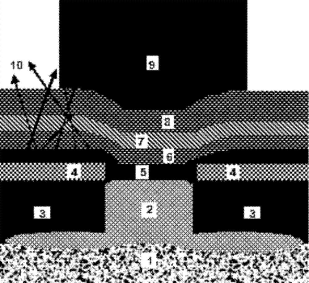
[0048] Such as figure 2 As shown, in the first embodiment, the hard mask film layer structure in the base region of the silicon germanium triode includes:

[0049] A silicon wafer 1 has a collector region 2 and a field isolation region 3 above it, and a polysilicon layer 4 and a silicon-germanium thin film layer 5 are grown on the collector region 2 and the field isolation region 3, wherein a part of the silicon-germanium thin film layer 5 is grown on An inorganic anti-reflection material layer 11 is grown above the polysilicon layer 4 and above the germanium-silicon film layer 5, and a second hard mask layer 7 is grown above the inorganic anti-reflection material layer 11, and the inorganic anti-reflection material layer 11 is used as a hard mask layer use.

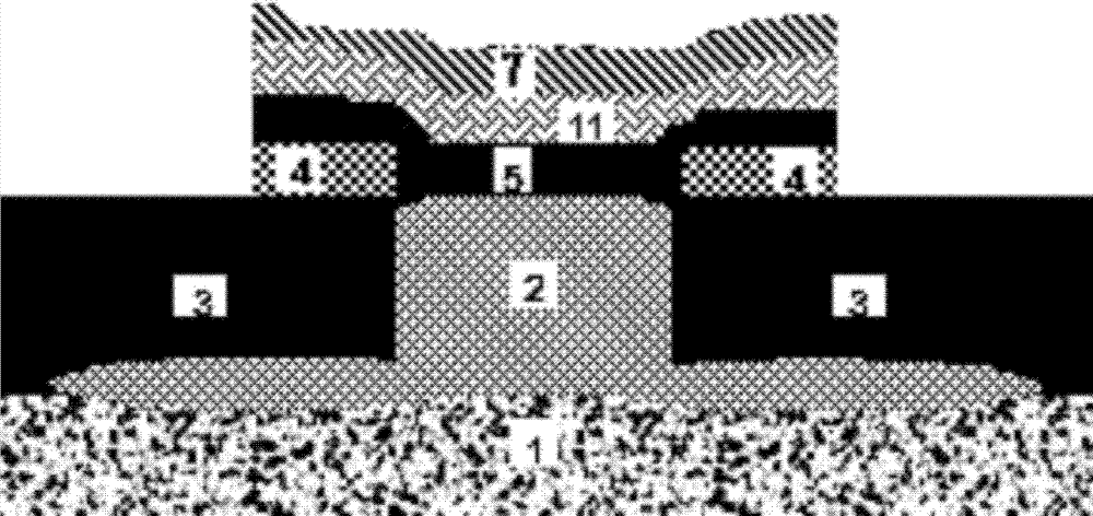
[0050] Such as image 3 As shown, in the second embodiment, the hard mask film layer structure in the base region of the silicon germanium triode includes:

[0051] A silicon chip 1 has a collector region 2 and a fie...


PUM


Abstract

The invention discloses a germanium-silicon triode base region hard mask membrane layer structure, which comprises a silicon chip, wherein a collector region and a field isolation region are arranged on the silicon chip; a polycrystalline silicon layer and a germanium-silicon membrane layer are grown on the collector region and the field isolation region, and the germanium-silicon membrane layer is partially grown above the polycrystalline silicon layer; and an inorganic anti-reflection material layer and at least one hard mask membrane layer are grown above the germanium-silicon membrane layer. The invention further discloses a manufacturing method of the germanium-silicon triode base region hard mask membrane layer structure. Through adoption of the germanium-silicon triode base region hard mask membrane layer structure, the influence of a germanium-silicon membrane layer diffuse reflection beam to the appearance of the photoresist is reduced, the control acpability to key sizes in the production is improved, and photoetching patterns of small sizes are obtained.

Description

technical field [0001] The invention relates to the field of semiconductor integrated circuit manufacturing, in particular to a hard mask film layer structure in the base region of a germanium-silicon triode. The invention also relates to a method for manufacturing the hard mask film layer structure of the base region of the silicon germanium triode. Background technique [0002] Such as figure 1 As shown, in the semiconductor Bi-polar (bipolar) or Bi-CMOS (bipolar CMOS) process, in order to improve the frequency and speed characteristics of the device, silicon germanium (SiGe, that is, doping germanium in silicon) process will be introduced to manufacture The base area of ​​the transistor (Base). Due to the existence of strain energy in the silicon germanium thin film layer, the surface of the silicon germanium thin film layer grown by epitaxial growth becomes very rough, and the diffuse reflection of light caused by the rough surface of the silicon germanium thin film la...

Claims


Application Information

Patent Timeline
Patent Type & Authority Patents(China)
IPC IPC(8): H01L29/73H01L29/06H01L21/331
Inventor 郭晓波孟鸿林
Owner SHANGHAI HUAHONG GRACE SEMICON MFG CORP
Why Eureka
Try Eureka