

Perovskite film, perovskite electroluminescence device and preparation method and display device
A technology of perovskite and perovskite materials, which is applied in the fields of electrical solid-state devices, chemical instruments and methods, semiconductor/solid-state device manufacturing, etc., and can solve the problems of film formation quality limitation, low turn-on voltage, brightness and current efficiency, etc.
- Summary
- Abstract
- Description
- Claims
- Application Information
AI Technical Summary
Problems solved by technology
Method used
Image

Examples
Embodiment 1
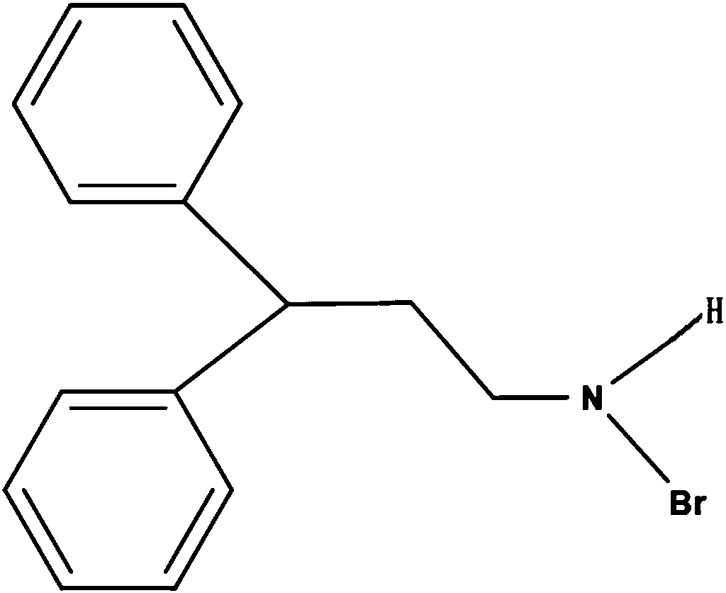
[0059] The present embodiment provides a perovskite thin film, comprising: a crystalline perovskite material on a substrate; and a halogenated amine ligand material grafted on the crystalline perovskite material.
[0060] Since the crystalline perovskite material in the perovskite film of this embodiment is grafted with a halogenated amine ligand material, the surface of the perovskite film is smooth, and the film surface coverage of the crystalline perovskite material is high , there is no obvious hole defect, and at the same time, because the halogenated amine ligand material is added in the perovskite film, the perovskite film in this embodiment has a very high fluorescence quantum yield (>70%). Moreover, since the halogenated amine ligand materials usually have good hydrophobic properties, the perovskite film has good stability in air.
[0061] In order to be more clear about the perovskite thin film in this embodiment, this embodiment also provides a preparation method fo...
Embodiment 2
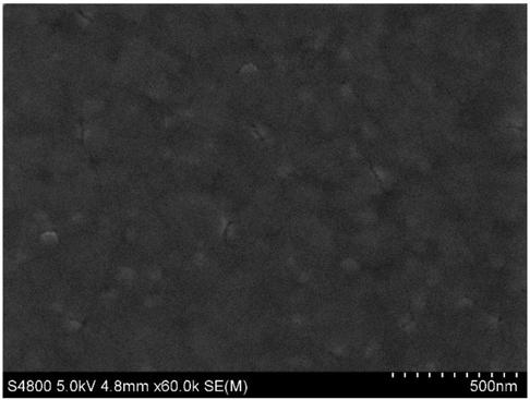
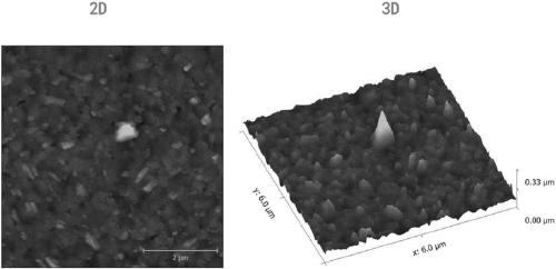
[0083] The present embodiment provides a perovskite thin film, comprising: a crystalline perovskite material on a substrate; and a halogenated amine ligand material grafted on the crystalline perovskite material. In particular, the crystalline perovskite material in the perovskite thin film of this embodiment includes perovskite nanocrystals and perovskite quantum dots, respectively as Figure 10 , 11 As shown, that is, the perovskite film in this embodiment is a composite film.
[0084] Since the crystalline perovskite material (including perovskite nanocrystals and perovskite quantum dots) in the perovskite composite film in this embodiment is grafted with a halogenated amine ligand material, the perovskite composite The surface of the film is smooth, and the surface coverage is high, and there is no obvious hole defect. At the same time, because there are a large number of perovskite quantum dot materials grafted with amine halide ligands in the perovskite composite film, ...
Embodiment 3
[0112] like Figure 15 As shown, a perovskite electroluminescent device is provided in this embodiment, including a cathode 2, an anode 1 disposed on a substrate 10, and a light-emitting layer 3 between the cathode 2 and the anode 1; wherein the light-emitting layer 3. The perovskite thin film in embodiment 1 or 2 can be used.
[0113] Since the light-emitting layer 3 of the perovskite electroluminescent device in this embodiment adopts the perovskite thin film in embodiment 1 or 2, the surface of the perovskite thin film is smooth, thereby effectively improving the brightness of the perovskite electroluminescent device and current efficiency. Especially when the perovskite film includes perovskite nanocrystals and perovskite quantum dots, that is, when the perovskite film is a composite film, the perovskite electroluminescent device can use the perovskite film to load at high speed. The characteristics of carrier transport speed, long diffusion length and ultra-high fluores...
PUM
| Property | Measurement | Unit |
|---|---|---|
| Half width | aaaaa | aaaaa |
| Particle size | aaaaa | aaaaa |
| Particle size | aaaaa | aaaaa |
Abstract
Description
Claims
Application Information