A superjunction reverse resistance type igbt with variable doping field stop layer

A technology of field stop layer and variable doping, which is applied in the direction of semiconductor devices, electrical components, circuits, etc., can solve the problems of low reverse withstand voltage and achieve bidirectional withstand voltage, good turn-off loss, and good conduction voltage drop Effect

Active Publication Date: 2020-07-31
UNIV OF ELECTRONICS SCI & TECH OF CHINA
View PDF5 Cites 0 Cited by
  • Summary
  • Abstract
  • Description
  • Claims
  • Application Information

AI Technical Summary

Problems solved by technology

However, since ordinary super-junction IGBT devices are not optimized for their reverse withstand voltage, their reverse withstand voltage is very low

Method used


Image

  • A superjunction reverse resistance type igbt with variable doping field stop layer
  • A superjunction reverse resistance type igbt with variable doping field stop layer
  • A superjunction reverse resistance type igbt with variable doping field stop layer

Examples


Embodiment Construction

[0016] The present invention is described in detail below in conjunction with accompanying drawing

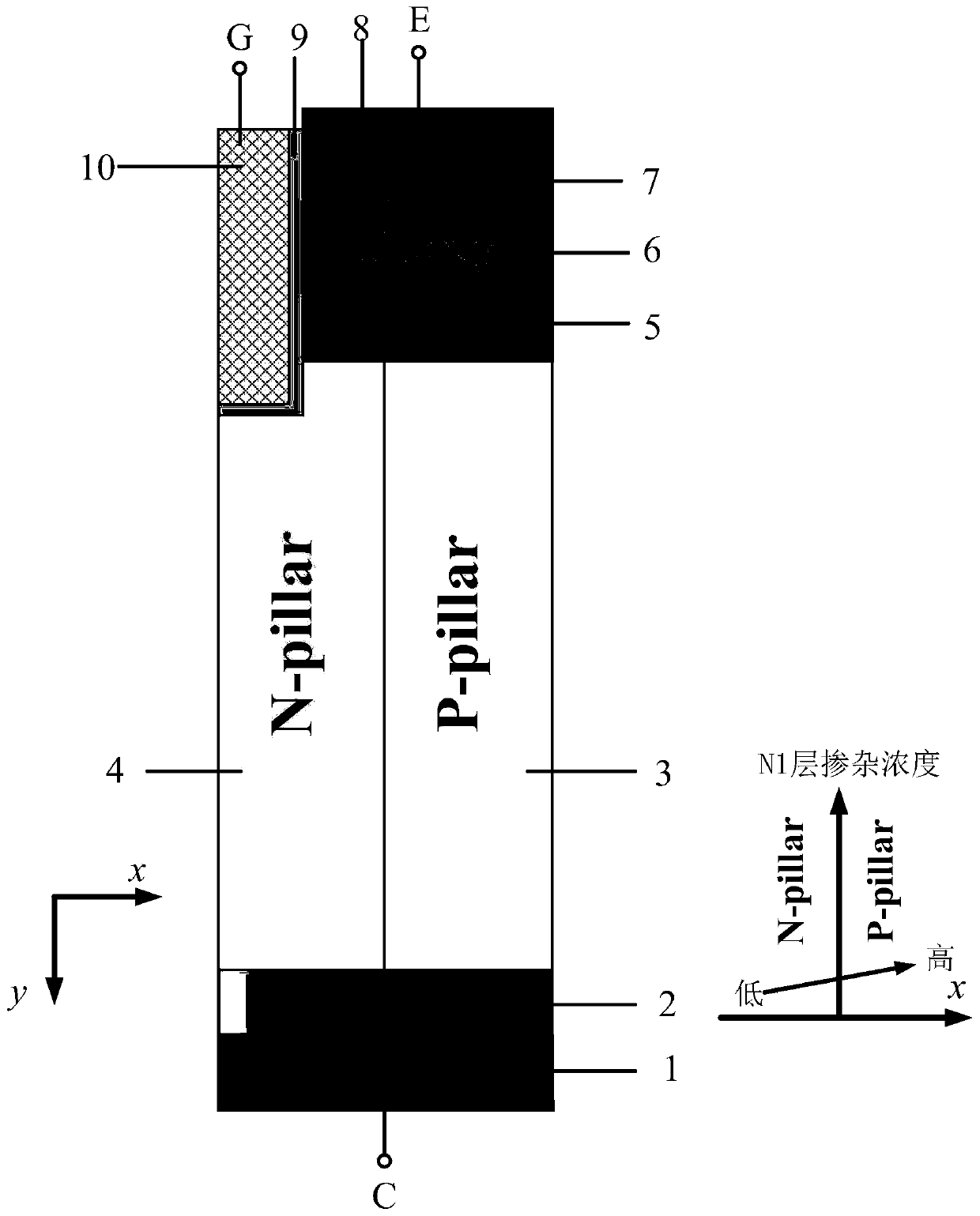
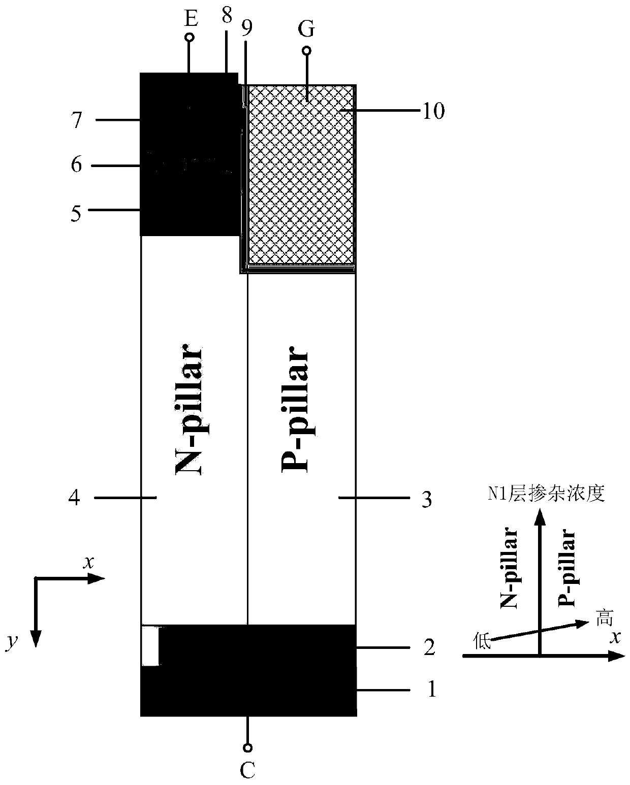
[0017] like figure 1 Shown is the reverse resistance IGBT with super junction of the present invention. It works as follows:

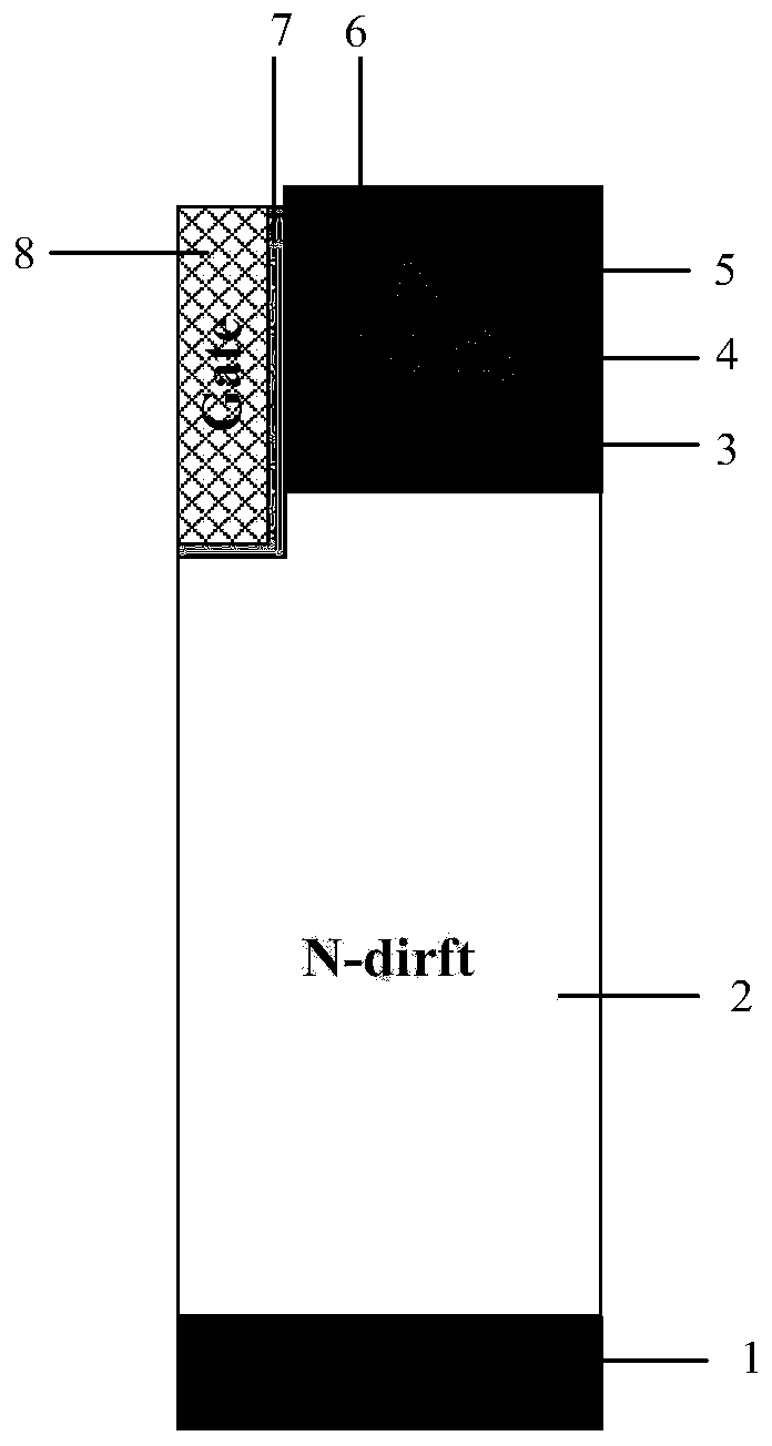
[0018] Figure 4 for figure 1 The simplified structure of the device of the present invention is used to analyze the electric field distribution when the device withstands voltage. Figure 5 When the collector is connected to the high voltage and the emitter is grounded, that is, when the device is forward withstand voltage, Figure 4 Electric field distribution diagram for a simplified structure. from Figure 5 It can be seen that the maximum electric field is on the J1 junction, and the electric field of the device is not uniformly distributed from point A to point B and from A' to B', and the electric field on the J2 junction is from A to B, that is, from near the N-type bar direction to the direction close to the P-type strip gradually decr...


PUM


Abstract

The invention relates to a power semiconductor technology, and particularly relates to a superjunction reverse-resistance IGBT with a variable doped field stop layer. Compared with a conventional superjunction reverse-resistance IGBT, the IGBT provided by the invention has the advantages that a superjunction structure is arranged in a drift region, and the concentration distribution of a first N-type layer is optimized: the concentration thereof gradually increases from left to right. The introduction of the superjunction structure makes an electric field in the drift region of the device in approximate rectangular distribution. Compared with the longitudinal electric field distribution of a conventional NPT reverse-resistance IGBT triangle, the same withstand voltage can be acquired in the shorter drift region length, thereby improving the compromise between the turn-on voltage drop of the device and the turn-off loss. According to the invention, the concentration distribution of thefirst N-type layer is optimized; punch-through of the first N-type layer is prevented when the device is at forward withstand voltage; and the first N-type layer can be completely depleted at the reverse withstand voltage and the peak electric field thereat is more uniform. The IGBT provided by the invention has the advantages that the bidirectional withstand voltage is realized, and the compromise between the turn-on voltage drop and the turn-off loss is optimized.

Description

technical field [0001] The invention belongs to the technical field of power semiconductors, in particular to a super junction reverse resistance IGBT (Insulated gate bipolar transistor, insulated gate bipolar transistor) with a variable doping field stop layer. Background technique [0002] The anti-resistance IGBT is a new type of power semiconductor device with positive and negative bidirectional blocking capabilities. Two anti-resistance IGBTs can be connected in antiparallel to form a bidirectional switch. The traditional bidirectional switch consists of two anti-parallel ordinary IGBTs and fast recovery diodes, which play an important role in the matrix inverter. Replacing the traditional bidirectional switch with the anti-resistance IGBT can not only reduce the conduction power consumption caused by the extra diode, but also reduce the volume of the system and the parasitic inductance in the system. [0003] The traditional reverse resistance IGBT uses NPT (Non-Punch...

Claims


Application Information

Patent Timeline
Patent Type & Authority Patents(China)
IPC IPC(8): H01L29/06H01L29/739
CPCH01L29/0634H01L29/7397H01L29/7398
Inventor 郑崇芝夏云谯彬李青岭孙瑞泽刘超施宜军信亚杰王方洲陈万军
Owner UNIV OF ELECTRONICS SCI & TECH OF CHINA
Why Eureka
Try Eureka