Reverse conducting IGBT without Snapback effect and manufacturing method thereof

A reverse conduction and effect technology, applied in semiconductor/solid-state device manufacturing, semiconductor devices, electrical components, etc., can solve the problems of forward and reverse conduction time asymmetry, and the requirements for reverse conduction characteristics of devices are not strict, and achieve forward conduction. Good pass characteristics, low cost, good soft recovery characteristics

Active Publication Date: 2019-11-01
UNIV OF ELECTRONICS SCI & TECH OF CHINA
View PDF5 Cites 2 Cited by
  • Summary
  • Abstract
  • Description
  • Claims
  • Application Information

AI Technical Summary

Problems solved by technology

[0006] The purpose of the present invention is to solve the problem of the snapback phenomenon existing in the forward conduction of the traditional RC-IGBT, and the situation that the requirements for the reverse conduction characteristics of the device are not strict due to the asymmetry of the forward and reverse conduction time of the device, and propose a Novel non-snapback effect reverse conduction IGBT and manufacturing method thereof

Method used


Image

  • Reverse conducting IGBT without Snapback effect and manufacturing method thereof
  • Reverse conducting IGBT without Snapback effect and manufacturing method thereof
  • Reverse conducting IGBT without Snapback effect and manufacturing method thereof

Examples


Embodiment Construction

[0059] The present invention is described in detail below in conjunction with accompanying drawing:

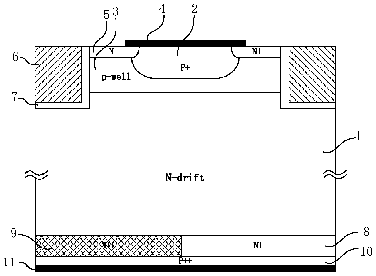
[0060] A new type of reverse conduction IGBT without snapback effect proposed by the present invention, its structure is as follows figure 1 As shown, it includes a collector structure, a drift region structure, an emitter structure and a gate structure; the collector structure includes a P++ collector region 10 and a metallized collector 10 located on the lower surface of the P++ collector region 10; the drift The region structure includes an N++ layer 9, an N+ field stop layer 8, and an N-drift region layer 1 located on the upper surface of the N++ layer 9 and the N+ field stop layer 8, and the N++ layer 8 and the N+ field stop layer 8 are arranged in parallel in the P++ collector region 10 The upper surface; the gate structure is a trench gate, which is embedded on the upper surface of the N-drift region layer 1, and its structure includes a gate oxide layer 7 and a polysil...


PUM


Abstract

The present invention relates to semiconductor technology, and more particularly to a reverse conducting IGBT without a Snapback effect and a manufacturing method thereof. The main scheme of the invention is that: the collector structure at the back surface of an IGBT is improved, the reverse blocking voltage of the device is reduced as much as possible by optimizing the doping concentration and the thickness of a P++ collector region and an N++ layer, and the reverse conduction is achieved by adopting the avalanche breakdown effect and the tunnel breakdown effect in the reverse blocking mode.Compared to a conventional reverse-conducting IGBT, since there is no an N+ short-circuit region, and there is no transition from an MOSFET conduction mode to an IGBT conduction mode during forward conduction, the snapback phenomenon cannot occur when the forward conducting of the new reverse-conducting IGBT provided by the invention is performed. Since the threshold voltage of the reverse conducting of the novel reverse conducting IGBT proposed by the present invention is larger than that of the conventional reverse conducting IGBT, the reverse conducting IGBT is suitable for a case that theforward conducting time is mostly occupied such as a quasi-resonant circuit and the reverse conducting time is short. Besides, the novel reverse conducting IGBT provide in the invention has the advantages such as the small forward voltage drop and good soft recovery characteristics.

Description

technical field [0001] The invention belongs to the technical field of power semiconductors, and relates to a reverse conduction IGBT without snapback effect and a manufacturing method thereof. Background technique [0002] Insulated gate bipolar transistor (IGBT) is a composite device developed in the 1980s. It uses MOSFET to drive bipolar transistors. It has the common advantages of MOSFET and BJT - high input impedance and low conduction voltage drop, so it is widely used Applied in medium frequency and medium power electrical. However, since the IGBT does not have the ability of reverse conduction, in the application of its inductive load, it is necessary to connect a Fast Recovery Diode (FRD for short) in reverse parallel to provide freewheeling protection. [0003] Since IGBT and FRD are easy to introduce parasitic inductance when soldering, it will cause high cost and poor reliability of the actual IGBT application. RC-IGBT) adopts a collector short-circuit structur...

Claims


Application Information

Patent Timeline
Patent Type & Authority Applications(China)
IPC IPC(8): H01L29/06H01L29/08H01L29/739H01L21/331
CPCH01L29/0684H01L29/0821H01L29/66348H01L29/7397H01L29/7398
Inventor 张波肖紫嫣陈万军周琪钧刘超谯彬
Owner UNIV OF ELECTRONICS SCI & TECH OF CHINA
Why Eureka
Try Eureka