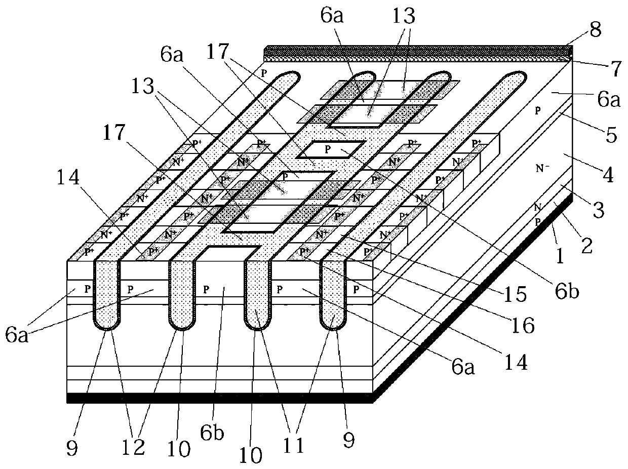
IGBT device structure

A device structure and contact window technology, applied in semiconductor devices, electrical components, circuits, etc., can solve the problems of inability to reduce the on-state voltage drop of the device, difficult to reduce the lithography alignment error, and low carrier concentration. The effect of reducing the difficulty of drawing, increasing the current density, and reducing the on-state voltage drop

Active Publication Date: 2019-11-05
NARI TECH CO LTD
View PDF2 Cites 3 Cited by
  • Summary
  • Abstract
  • Description
  • Claims
  • Application Information

AI Technical Summary

Problems solved by technology

It has the following defects: when the device is turned off, the carrier concentration accumulated under the trench region is too low, resulting in the on-state voltage drop of the device cannot be reduced; with the development of the process, the width of the dummy trench is also designed to be wider and wider. Narrower and narrower, its width can be less than 1.5 μm, the polysilicon width in the virtual trench is narrower, when the contact window connecting the metal emitter and the structure below the contact window is opened from the middle of the virtual trench polysilicon, the position accuracy error of the contact window very strict
The long-term high-temperature process will inevitably cause the wafer to warp under the action of thermal stress, making it difficult to reduce the alignment error of lithography, which is a very difficult problem to solve

Method used


Image

  • IGBT device structure

Examples


Embodiment Construction

[0014] The present invention will be further described below in conjunction with the accompanying drawings. The following examples are only used to illustrate the technical solution of the present invention more clearly, but not to limit the protection scope of the present invention.

[0015] It should be noted that, in the description of the present invention, the terms "front", "rear", "left", "right", "upper", "lower", "inner", "outer" and the like indicate orientations or positions The relationship is based on the orientation or positional relationship shown in the drawings, and is only for the convenience of describing the present invention and does not require that the present invention must be constructed and operated in a specific orientation, and thus should not be construed as a limitation of the present invention. The terms "front", "rear", "left", "right", "upper" and "lower" used in the description of the present invention refer to the directions in the drawings, ...


PUM


Abstract

The invention discloses an IGBT device structure in the technical field of power semiconductor devices, aims to solve the technical problems that in the prior art, when an IGBT device adopting a virtual trench gate structure is turned off, the on-state voltage drop of a device cannot be reduced due to the fact that the concentration of carriers accumulated below a trench region is too low, and thedifficulty of opening a contact window from the middle of virtual trench polycrystalline silicon is increased as the width of a virtual trench is designed to be narrower and narrower. The top surfaceof the device is downwards provided with a plurality of active trenches and virtual trench regions which are distributed at intervals. Each virtual trench region comprises at least one bridge and a plurality of virtual trenches connected through the bridge, and a dielectric layer is provided with a contact window; and P-type well regions comprise a first P-type well region connected with the metal emitter through the contact window and a second P-type well region in a potential floating state.

Description

technical field [0001] The invention relates to an IGBT device structure, belonging to the technical field of power semiconductor devices. Background technique [0002] As a new type of power semiconductor device, IGBT has the advantages of high withstand voltage characteristics and low on-resistance, and also has the characteristics of simple gate control, high input impedance, fast switching speed, high current density, and saturation voltage drop. A new generation of mainstream products. [0003] At present, many IGBT devices adopt a dummy trench gate structure. The IGBT device adopting the virtual trench gate structure includes a virtual trench, and a strip-shaped contact window parallel to the strip-shaped trench gate is provided on the polysilicon of the virtual trench. It has the following defects: when the device is turned off, the carrier concentration accumulated under the trench region is too low, resulting in the on-state voltage drop of the device cannot be re...

Claims


Application Information

Patent Timeline
Patent Type & Authority Applications(China)
IPC IPC(8): H01L29/06H01L29/739
CPCH01L29/0684H01L29/0603H01L29/7397H01L29/7398
Inventor 郑婷婷李宇柱李伟邦骆健董长城
Owner NARI TECH CO LTD
Why Eureka
Try Eureka