High withstand voltage and low loss super junction power device

A power device and drift region technology, applied in semiconductor devices, electrical components, circuits, etc., can solve problems such as blocking voltage drop, and achieve the effect of low forward voltage drop and high forward blocking voltage

Active Publication Date: 2019-11-05
UNIV OF ELECTRONIC SCI & TECH OF CHINA
View PDF3 Cites 5 Cited by
  • Summary
  • Abstract
  • Description
  • Claims
  • Application Information

AI Technical Summary

Problems solved by technology

However, in the blocking state, the potential of the P column will increase with the increase of the collector voltage, and the electric force lines emitted by the ionized donor impurities in the N column area will tend to terminate i

Method used


Image

  • High withstand voltage and low loss super junction power device
  • High withstand voltage and low loss super junction power device
  • High withstand voltage and low loss super junction power device

Examples


Example Embodiment

[0027] Example 1

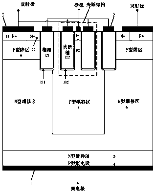
[0028] Such as image 3 A super junction insulated gate bipolar transistor is shown, including a collector structure, a drift region, an emitter structure, a trench gate structure, and a pinch-off structure, wherein the drift region is located on the collector structure, the emitter structure, and the trench gate structure And the pinch-off structure is located above the drift zone;

[0029] The collector structure includes a P-type collector layer 4 and an N-type buffer layer 5 on the upper surface of the P-type collector layer 4; the collector electrode 1 is drawn from the lower surface of the P-type collector layer 4;

[0030] The drift region includes an N-type drift region 6 and a P-type drift region 7, and the P-type drift region 7 and the N-type drift region 6 form a super junction structure or a semi-super junction structure;

[0031] The emitter structure includes a P-type well region 8 located on an N-type drift region. The upper part of the P-type well re...

Example Embodiment

[0036] Example 2

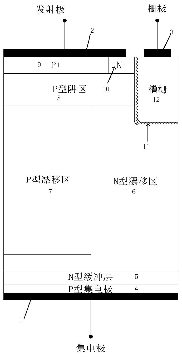
[0037] Such as Figure 4 As shown, the difference between this embodiment and Embodiment 1 is that this embodiment has a carrier storage layer 13 for blocking holes, and the carrier storage layer 13 is in contact with the lower surface of the P-type well region 8. N The upper surface of the type drift region 6 is in contact with the carrier storage layer 13; its working mechanism is the same as that of Embodiment 1. The added carrier storage layer further prevents holes from being collected by the emitter and reduces the forward conductivity. Through pressure drop.

Example Embodiment

[0038] Example 3

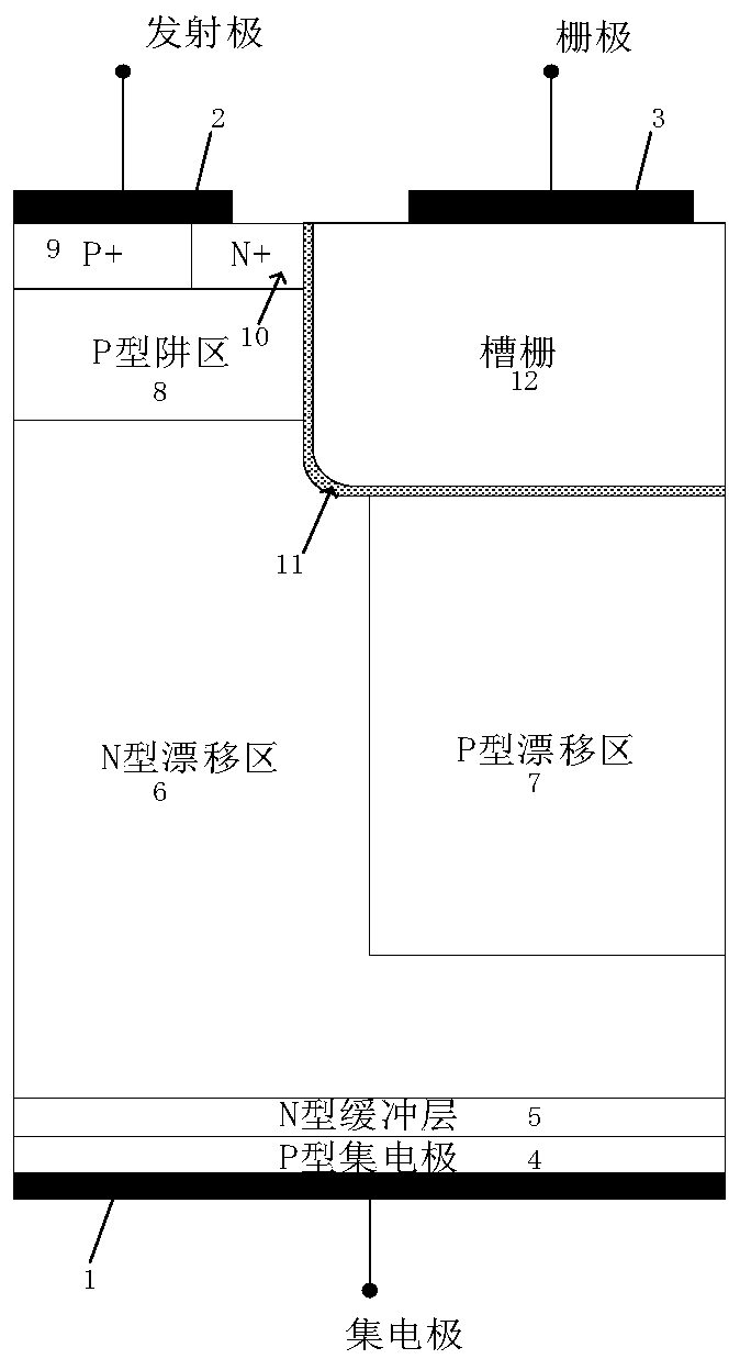
[0039] Such as Figure 5 As shown, the difference between this example and any one of Example 1 and Example 2 is that this example has three or more pinch-off grooves side by side in the pinch-off structure and the P-type body contact area 92 between the pinch-off grooves; its working mechanism Same as in Example 1 or Example 2, the added pinch-off structure allows more holes to extract paths and lower turn-off loss.


PUM


Abstract

The invention belongs to the technical field of power semiconductors, and in particular relates to a high withstand voltage and low loss super junction power device. The device provided by the invention is characterized in that a pinch-off structure is arranged on a P-type drift region; the pinch-off structure is composed of pinch-off grooves and a P-type body contact region between the pinch-offgrooves; during forward conduction, the pinch-off structure pinches the middle P-type drift region, suppressing the collection of holes by the P-type drift region and improving the storage effect of carriers in the drift region; when the device is turned off, the P-type drift region is connected with an emitter through the P-type body contact region to be used as a hole extraction path to reduce the turn-off loss; when forward withstand voltage is applied, the P-type drift region contacts the emitter through the P-type body contact region, and the potential is 0; the P-type drift region has abetter auxiliary depletion effect; and the device has higher withstand voltage. Compared with a conventional super junction IGBT device, the device provided by the invention has lower on-voltage dropand better Von-Eoff discount. Compared with a P-column floating super junction IGBT device, the super junction IGBT device provided by the invention have higher forward withstand voltage.

Description

Technical field [0001] The invention belongs to the field of semiconductor technology, in particular to a super junction power device with high withstand voltage and low loss. Background technique [0002] Insulated Gate Bipolar Transistor (IGBT) is a widely used semiconductor power device. It combines the advantages of high MOSFET input impedance and simple driving, as well as the advantages of high current density and reduced conduction voltage of BJT devices. The super junction is a withstand voltage structure in which the N-pillar region and the P-pillar region are alternately arranged. It can make the N-pillar region and the P-pillar region obtain a higher breakdown voltage even at a higher doping concentration. [0003] In the traditional super-junction IGBT, due to the large junction area of ​​the N-pillar region and the P-pillar region, the minority carrier holes injected from the P-type collector into the N-pillar region are easily drawn away by the P-pillar and flow into...

Claims


Application Information

Patent Timeline
IPC IPC(8): H01L29/739H01L29/06
CPCH01L29/0634H01L29/7397
Inventor 罗小蓉张森苏伟邓高强樊雕宋旭李聪聪魏杰
Owner UNIV OF ELECTRONIC SCI & TECH OF CHINA
Why Eureka
Try Eureka