Silicon-based near-infrared single photon avalanche diode detector and manufacturing method thereof

A single-photon avalanche and near-infrared technology, applied in the field of photoelectric detection, can solve the problems of reducing the size of the device, dark count noise, low near-infrared photon detection efficiency, etc. wide effect

Inactive Publication Date: 2019-11-05
NANJING UNIV OF POSTS & TELECOMM
View PDF12 Cites 22 Cited by
  • Summary
  • Abstract
  • Description
  • Claims
  • Application Information

AI Technical Summary

Problems solved by technology

[0006] Purpose of the invention: The purpose of the present invention is to provide a silicon-based near-infrared single-photon avalanche diode detector. Aiming at the low detection efficiency of the traditional silicon-based integrated single-photon avalanche diode detector for near-infrared photons, the N+ buried The deep PN junction formed between the layer and the deep P well is used as the avalanche region of the device, and the low-doped and uniformly distributed P-type epitaxial layer is used as a virtual guard ring to improve the detection efficiency of near-infrared photons, reduce the size of the device and reduce the dark count noise

Method used


Image

  • Silicon-based near-infrared single photon avalanche diode detector and manufacturing method thereof
  • Silicon-based near-infrared single photon avalanche diode detector and manufacturing method thereof
  • Silicon-based near-infrared single photon avalanche diode detector and manufacturing method thereof

Examples


Embodiment 1

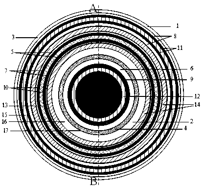
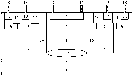
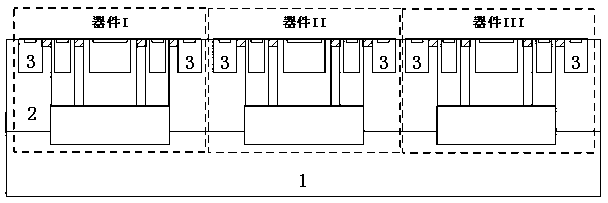
[0045] Specific dimensions of the single photon avalanche diode detector: the overall device is 11 μm long and 9 μm deep. Among them, the local heavily doped N+ buried layer region 2 directly above the P-type substrate 1 and between the P-type epitaxial layer region 3 is 8 μm long, the deep P well region 4 is 4 μm long, the central shallow P well region 6 is 3.8 μm long, and the central P+ The length of region 9 is 3.5 μm, the length of deep N well region 5 is 1 μm, the length of shallow N well region 7 is 0.8 μm, the length of N+ region 10 is 0.4 μm, the length of shallow trench isolation region 14 on the left and right sides of N+ region 10 is 0.4 μm, and the length of anode 12 is 0.5 μm, the length of the cathode 13 is 0.5 μm, and the length of the ground electrode 15 is 0.5 μm (the above-mentioned lengths are all the transverse lengths of the cross-section of the detector); the virtual guard ring region 16 between the deep P well region and the deep N well regions on both s...


PUM


Abstract

The invention discloses a silicon-based near-infrared single photon avalanche diode detector, and belongs to the technical field of photoelectric detection. The single photon avalanche diode detectorcomprises a P-type epitaxial layer arranged above a P-type substrate, wherein the P-type substrate and the P-type epitaxial layer are provided with an N+ buried layer region therebetween, deep P wellregions are symmetrically arranged on the N+ buried layer region, a deep P well region is arranged on the N+ buried layer region at the central position, and an avalanche region is formed between thedeep P well region and the N+ buried layer region. According to the single photon avalanche diode detector, the deep avalanche region is formed between the deep P well and the N+ buried layer, the lightly-doped and uniformly distributed P-type epitaxial layer is utilized as a virtual protection ring at the same time to improve the near-infrared photon detection efficiency, the size of the device is reduced, and the dark counting noise is reduced. The manufacturing method can carry out manufacturing based on the standard silicon-based process, and has the advantages of low cost, high integration, low power consumption, near-infrared detection capability and the like.

Description

technical field [0001] The invention belongs to the technical field of photoelectric detection, and in particular relates to a silicon-based near-infrared single-photon avalanche diode detector and a manufacturing method thereof. Background technique [0002] Single photon avalanche photodiodes (ie: single photon avalanche diodes, SPAD) have the characteristics of fast response, large avalanche gain, high detection efficiency, small size, light weight, and low power consumption, and have become the best device for making single photon detectors. . [0003] The SPAD detector can detect very weak photons (up to the order of single photons), and sample and calculate the light field of the imaging target in time and space, and finally obtain the required high-quality imaging results, so it is used in quantum communication , astronomical detection, biological waveguide, radiation detection, high-energy physics, astronomical photometry, optical time-domain reflectometry and quant...

Claims


Application Information

Patent Timeline
Patent Type & Authority Applications(China)
IPC IPC(8): H01L31/0352H01L31/028H01L31/107H01L31/18
CPCH01L31/028H01L31/035272H01L31/107H01L31/18Y02P70/50
Inventor 徐跃孙飞阳
Owner NANJING UNIV OF POSTS & TELECOMM
Why Eureka
Try Eureka