Chemical vapor deposition device and method

A chemical vapor deposition and heating device technology, which is applied in gaseous chemical plating, metal material coating process, coating, etc., can solve the problems of low growth rate and poor film growth consistency, and achieve simplified process, reduced processing cost, Effects that increase controls and abilities

Active Publication Date: 2019-11-12
左然 +1
View PDF8 Cites 8 Cited by
  • Summary
  • Abstract
  • Description
  • Claims
  • Application Information

AI Technical Summary

Problems solved by technology

[0012] The purpose of the present invention is to provide a chemical vapor deposition device and method for the above problems, which can effectively avoid the problems of gas phase parasitic reaction, cross-contamination, low growth rate and poor film growth consistency in film growth, and can isolate different reaction precursors, and achieve rapid heating and cooling and gas switching

Method used


Image

  • Chemical vapor deposition device and method
  • Chemical vapor deposition device and method
  • Chemical vapor deposition device and method

Examples


Embodiment 1

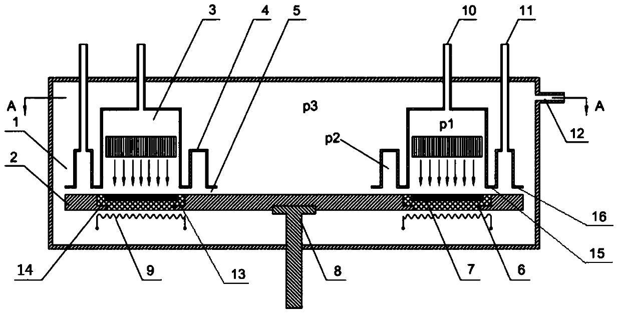
[0049] Such as figure 1 , 2 and 3, figure 1 It is a schematic structural diagram of a chemical vapor deposition device provided by the present invention, figure 2 It is a schematic top view of a structure of the chemical vapor deposition device provided by the present invention after removing the outer cavity, image 3 It is a schematic top view of another structure of the chemical vapor deposition device provided by the present invention after removing the outer cavity. The chemical vapor deposition device includes an outer cavity 1, a moving tray 2, an inner cavity 3, an exhaust cavity 4, a tray groove 14, a wafer loading area 6, a heating device 9, a gas supply pipeline 10, a second An exhaust duct 11 and a second exhaust duct 12;

[0050] The outer cavity 1 is a cylindrical airtight cavity structure; the moving tray 2 is thin cylindrical, the diameter of the moving tray 2 is slightly smaller than the diameter of the outer cavity 1, and the moving tray 2 is horizontall...

Embodiment 2

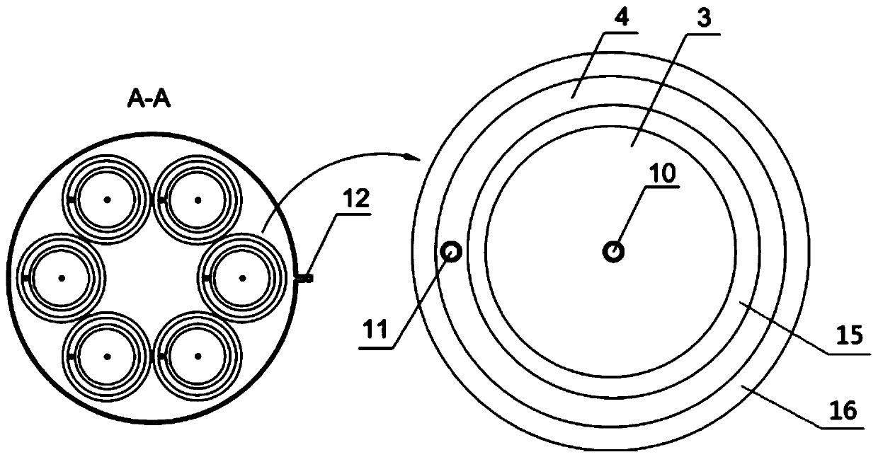
[0076] Such as Figure 4 Shown is one embodiment of the chemical vapor deposition apparatus of the present invention. The moving tray 2 is indexed and rotated between the inner cavity 3a and the inner cavity 3b, and the wafers 7 that are separately arranged on each wafer loading area 6 on the upper surface of the moving tray 2 stay in different inner cavities 3a or 3b for a while in turn, The reaction precursor in the inner chamber 3a and the purge gas in the inner chamber 3b are received alternately, with a typical residence time of 1-5 seconds. For example, the wafer carrying area 6 first passes through the inner cavity 3 for transporting the Group III precursor, and the surface adsorbs the Group III precursor; 2 The inner cavity 3 of the group III gas-phase precursor is purged away, leaving only the surface adsorbed particles; and then the group V precursor is continuously adsorbed on the surface of the group III precursor through the inner cavity 3 of the group V; Finall...

Embodiment 3

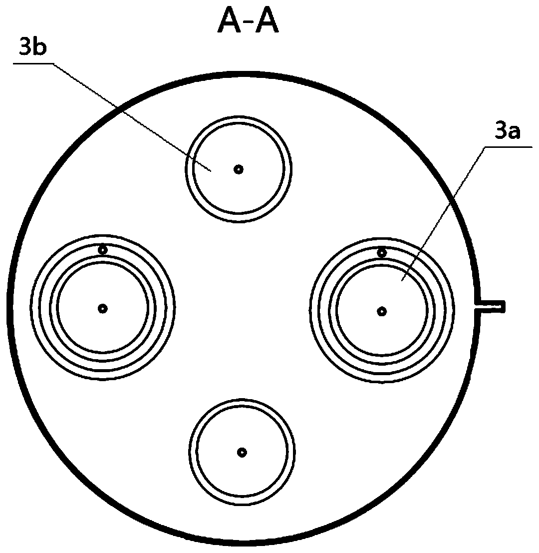
[0078] Such as Figure 5 Shown is another embodiment of the chemical vapor deposition apparatus of the present invention. The introduction of inert gas into the inner chamber 3 is canceled, and only the reaction precursor is introduced into the inner chamber 3 . The moving tray 2 is indexed and rotated among a plurality of inner cavities 3 , and the wafers arranged on each wafer carrying area 6 on the upper surface of the moving tray 2 pass through different inner cavities 3 in turn, but do not stay. Due to the lack of inert gas purge, when the wafer 7 is switched from one cavity 3 to another, the boundary layer above the surface of the wafer 7 will carry a small amount of the reaction precursor of the previous cavity 3 . Due to the capillary isolation between the inner chamber 3 and the outer chamber 1, the amount of the former reaction precursor in the gas phase above the wafer 7 is very small, and there is still only one reaction precursor, thus greatly reducing the gas ph...


PUM


Abstract

The invention provides a chemical vapor deposition device and method. The chemical vapor deposition device comprises an outer cavity body, a motion tray, inner cavity bodies, gas exhausting cavity bodies, tray grooves, chip bearing zones, heating devices, gas supply pipelines, first gas exhausting pipelines and a second gas exhausting pipeline; the same or different reaction precursor gases or inert gases are injected into the multiple independent inner cavity bodies, and through sealing of capillary gaps between the inner cavity bodies and the upper surface of the tray, the pressure intensityof the inner cavity bodies is always higher than that of the outer cavity body; and each inner cavity body is independently subjected gas feeding and gas exhausting, and independently heated and cooled; by controlling the motion tray to continuously rotate or rotate in an indexing mode, reaction precursors sprayed by nozzles in the different inner cavity bodies can be sprayed onto chips arrangedon the chip bearing zones on the upper surface of the motion tray by turns, and continuous chemical vapor deposition or periodic atomic layer deposition of a film is achieved. According to the chemical vapor deposition device and method, the different reaction precursors can be isolated, quick temperature raising, temperature lowering and gas switching are achieved, and the semiconductor film growing yield and productive rate are advantageously increased.

Description

technical field [0001] The invention belongs to the technical field of semiconductor equipment, and in particular relates to a chemical vapor deposition device and method. Background technique [0002] Chemical vapor deposition CVD is a key process for preparing semiconductor thin film devices, including solar thin film batteries, blue-violet LEDs, high-power power electronic devices and two-dimensional materials. CVD reactor is the key equipment to realize the above process. Most of the current CVD growth is to carry the more volatile reaction precursors into the reaction chamber through the carrier gas such as hydrogen or nitrogen, and use high temperature or plasma to activate the chemical reaction to achieve thin film deposition and grow thin film heterojunctions that meet the device requirements. . [0003] In order to obtain uniform film composition, thickness, and high growth rate, most of the existing film growth processes need to heat the wafer to a high temperatu...

Claims


Application Information

Patent Timeline
Patent Type & Authority Applications(China)
IPC IPC(8): C23C16/455C23C16/458C23C16/44
CPCC23C16/45551C23C16/45557C23C16/4584C23C16/4412
Inventor 左然陈景升
Owner 左然
Why Eureka
Try Eureka