
SoC chip deep sleep wake-up device

A deep sleep and wake-up device technology, applied in the direction of program control devices, program control design, instruments, etc., can solve the problem of inability to achieve ultra-low power consumption

Inactive Publication Date: 2019-11-12
SHENZHEN BETTERLIFE ELECTRONICS SCI & TECH
View PDF3 Cites 1 Cited by
  • Summary
  • Abstract
  • Description
  • Claims
  • Application Information

AI Technical Summary

Problems solved by technology

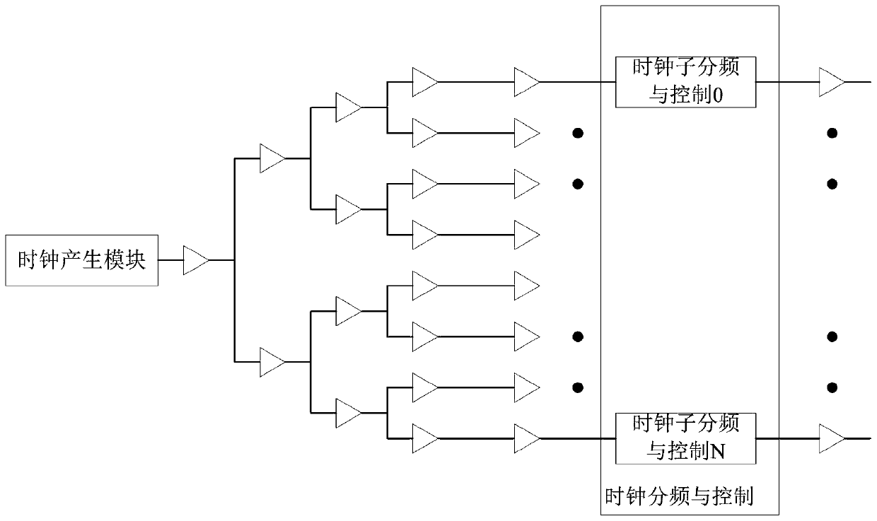
In the SoC chip, the clock tree network is often one of the largest sources of power consumption. Whether it is MCU sleep wake-up, or fingerprint / touch detection wake-up, the clock from the clock generation module to the clock control and frequency division module in the sleep state The tree network is working, and at the same time, some detection modules and interface modules are also working, so these two kinds of sleep are shallow sleep, which can reduce some power consumption, but cannot achieve ultra-low power consumption

Method used


Image

  • SoC chip deep sleep wake-up device
  • SoC chip deep sleep wake-up device
  • SoC chip deep sleep wake-up device

Examples


Embodiment Construction

[0030] The present invention will be described in more detail below in conjunction with the accompanying drawings and embodiments.

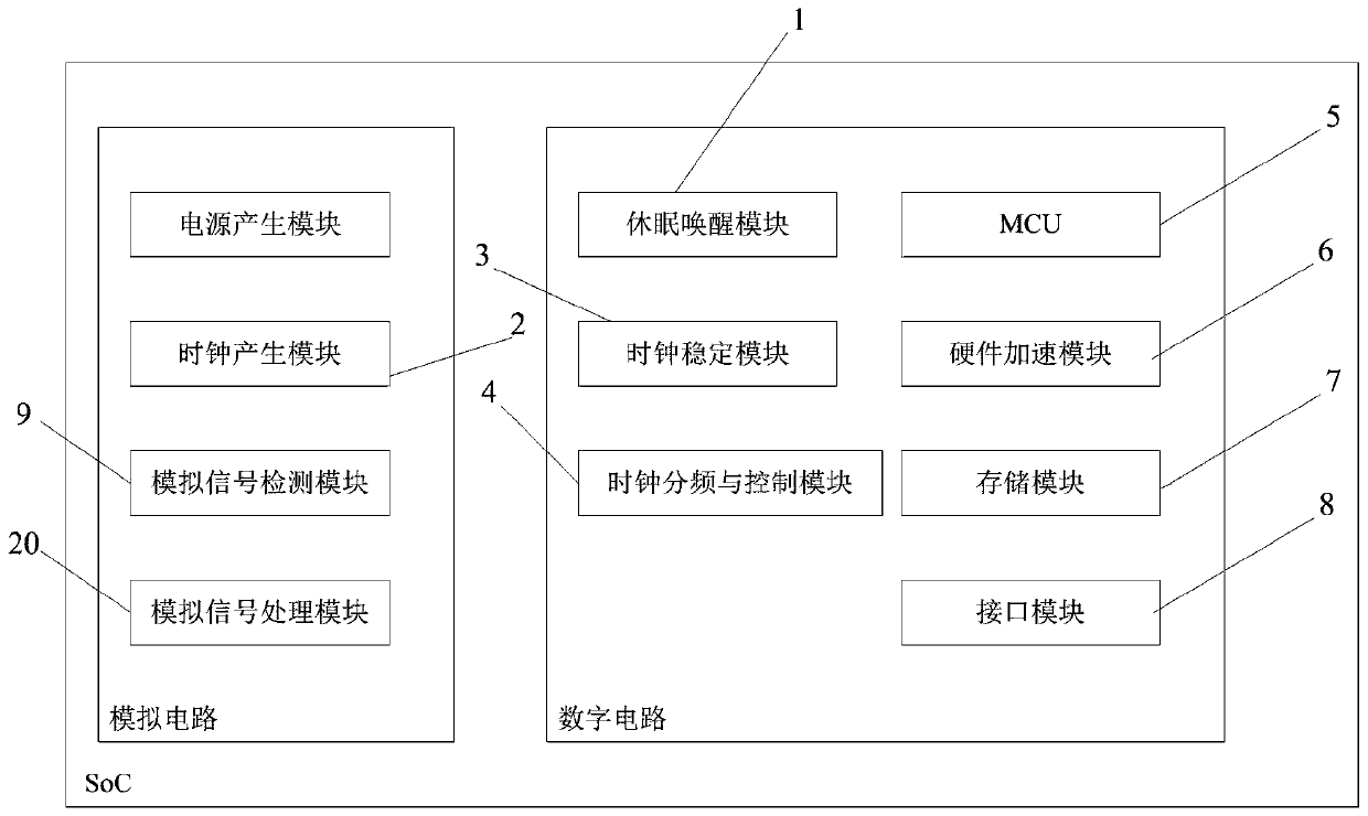
[0031] The invention discloses a SoC chip deep sleep wake-up device, please refer to image 3 and Figure 4 , which includes:

[0032] A dormant wake-up module 1, configured to access an external wake-up signal, generate an internal wake-up signal according to the external wake-up signal, and generate a source clock enable signal when the internal wake-up signal meets a preset wake-up requirement;

[0033] A clock generation module 2, connected to the dormancy wake-up module 1, the clock generation module 2 is used to generate a source clock signal according to the source clock enable signal;

[0034] A clock stabilization module 3, connected to the clock generation module 2, the clock stabilization module 3 is used for cumulatively counting the source clock signal, and generating a stable clock signal when the cumulative count value reaches a ...


PUM


Abstract

The invention discloses an SoC chip deep sleep wake-up device which comprises: a sleep wake-up module used for accessing an external wake-up signal, generating an internal wake-up signal according tothe external wake-up signal, and generating a source clock enable signal when the internal wake-up signal meets a preset wake-up requirement; a clock generation module which is used for generating a source clock signal according to the source clock enable signal; a clock stabilizing module which is used for carrying out accumulation counting on the source clock signal and generating a stable clocksignal after an accumulation counting value reaches a preset threshold value; and a clock frequency division and control module which is used for carrying out frequency division processing on the stable clock signal and then generating a plurality of clock signals capable of being used for working of an internal function module of the SoC chip. A two-stage awakening mechanism is adopted, clock signals do not need to participate in the dormancy awakening process, mistaken awakening can be avoided, and power consumption of a clock network can be avoided during dormancy.

Description

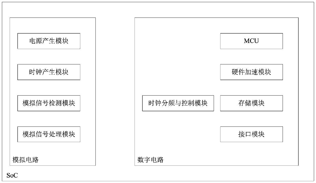
technical field [0001] The present invention relates to a SoC chip dormancy wake-up method, in particular to a SoC chip deep sleep wake-up device and method. Background technique [0002] One or more SoC (System on Chip, System on Chip) chips are usually integrated in a mobile electronic terminal. Due to the limited capacity of the battery, in order to increase the usage time of the mobile electronic terminal, the low power consumption control of the SoC chip has higher and higher requirements. [0003] For a typical structure of a SoC chip in the prior art, please refer to figure 1 , including the analog circuit part and the digital circuit part. The analog circuit part includes power generation module, clock generation module, analog signal detection module, and analog signal processing module, and the digital circuit part includes clock frequency division and control module, MCU, hardware acceleration module, storage module and interface module. One of the SoC sleep wa...

Claims


Application Information

Patent Timeline
IPC IPC(8): G06F15/78G06F9/4401
CPCG06F9/4418G06F15/7807Y02D10/00
Inventor 张弛张敏余佳
Owner SHENZHEN BETTERLIFE ELECTRONICS SCI & TECH
Learn More