Display panel and display device

A display panel and plane technology, applied in the direction of identification devices, instruments, electrical components, etc., can solve the thermal mismatch between the driving backplane and the substrate of the light-emitting device, the warping of the epitaxial layer wafer of the light-emitting device, and the influence of welding on both sides of the electrode Yield and other issues, to achieve the effect of weakening the quantum confinement Tasker effect, improving luminous brightness, and reducing the impact of binding yield

Active Publication Date: 2019-11-12
CHENGDU VISTAR OPTEOLECTRONICS CO LTD
View PDF7 Cites 6 Cited by
  • Summary
  • Abstract
  • Description
  • Claims
  • Application Information

AI Technical Summary

Problems solved by technology

[0003] The traditional bonding process uses solder to bond the electrodes on both sides, but the epitaxial layer of the light-emitting device has the problem of wafer warpage, which affects the welding yield of the electrodes on both sides, and the backplane and the substrate of the light-emitting device are driven during bonding. There is a problem of thermal mismatch at the bottom, which leads to the misalignment of electrodes on both sides, which further reduces the bonding yield

Method used


Image

  • Display panel and display device
  • Display panel and display device
  • Display panel and display device

Examples


Embodiment Construction

[0040] The present invention will be further described in detail below in conjunction with the accompanying drawings and embodiments. It should be understood that the specific embodiments described here are only used to explain the present invention, but not to limit the present invention. In addition, it should be noted that, for the convenience of description, only some structures related to the present invention are shown in the drawings but not all structures. Throughout this specification, the same or similar reference numerals represent the same or similar structures, elements or processes. It should be noted that, in the case of no conflict, the embodiments in the present application and the features in the embodiments can be combined with each other.

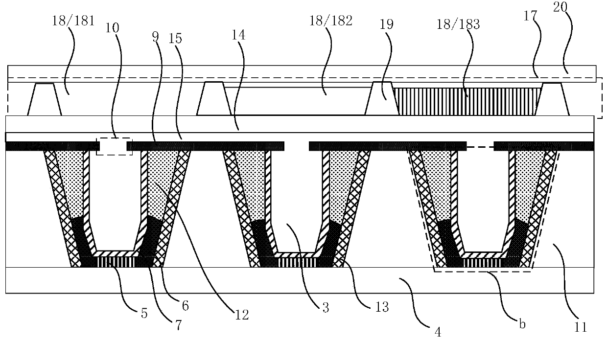
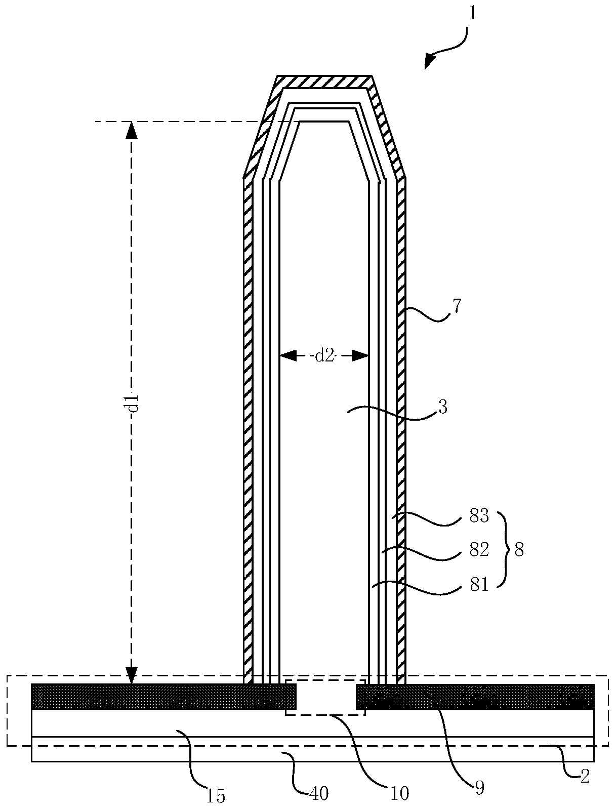
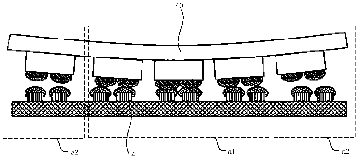
[0041] figure 1 It is a schematic cross-sectional structure diagram of a display panel provided by an embodiment of the present invention, figure 2 It is a schematic cross-sectional structure diagram of a light emitt...


PUM


Abstract

The invention discloses a display panel and a display device. The display panel comprises a plurality of light-emitting devices each of which comprises a planar film layer and a columnar structure protruding from the planar film layer; and a driving backplane provided with bonding pad corresponding to the light-emitting devices one to one and covered by a flexible conductive structure, wherein thecolumnar structures of the light-emitting devices are inserted into the flexible conductive structure to electrically connect metal electrodes wrapping the columnar structures with the correspondingbonding pads. The display panel greatly reduces the influence of wafer warpage on the binding yield, and avoids the binding misalignment caused by the thermal mismatch between the driving backplane and the light-emitting device substrate.

Description

technical field [0001] Embodiments of the present invention relate to the field of display technology, and in particular, to a display panel and a display device. Background technique [0002] Micro LED (Micro Light Emitting Diode, miniature light-emitting diode) will miniaturize and matrix the traditional LED, and is known as the next-generation display technology. With the advantages of fast response speed and large contrast ratio, the brightness is 30 times higher than that of OLED (Organic Light Emitting Diode, organic light emitting diode), and the power consumption is only about 10% of LCD (Liquid Crystal Display, liquid crystal display), which is 50% of OLED . [0003] The traditional bonding process uses solder to bond the electrodes on both sides, but the epitaxial layer of the light-emitting device has the problem of wafer warpage, which affects the welding yield of the electrodes on both sides, and the backplane and the substrate of the light-emitting device are ...

Claims


Application Information

Patent Timeline
Patent Type & Authority Applications(China)
IPC IPC(8): H01L27/15G09F9/33
CPCH01L27/156G09F9/33
Inventor 樊腾崔霜郭恩卿李之升王程功王雪丹李庆杨婷慧翟峰
Owner CHENGDU VISTAR OPTEOLECTRONICS CO LTD
Why Eureka
Try Eureka