Array substrate and manufacturing method thereof

An array substrate and glass substrate technology, applied in the display field, can solve the problems of decreased process yield, increased time, material cost, etc., and achieves the effect of saving process time, reducing the number of uses, and having a simple and reasonable structure

Active Publication Date: 2019-11-12
SHENZHEN CHINA STAR OPTOELECTRONICS SEMICON DISPLAY TECH CO LTD
View PDF6 Cites 9 Cited by
  • Summary
  • Abstract
  • Description
  • Claims
  • Application Information

AI Technical Summary

Problems solved by technology

As we all know, each additional process step will not only increase time and material costs, but also bring the risk of process yield decline

Method used


Image

  • Array substrate and manufacturing method thereof
  • Array substrate and manufacturing method thereof
  • Array substrate and manufacturing method thereof

Examples


Embodiment Construction

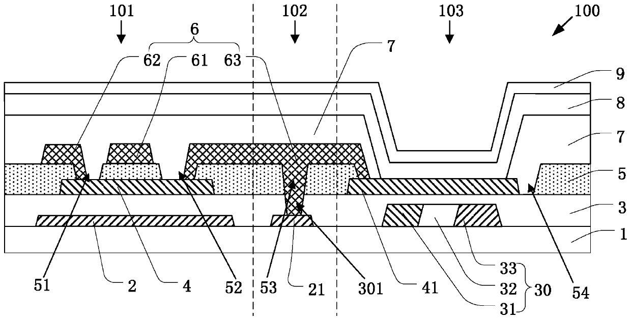
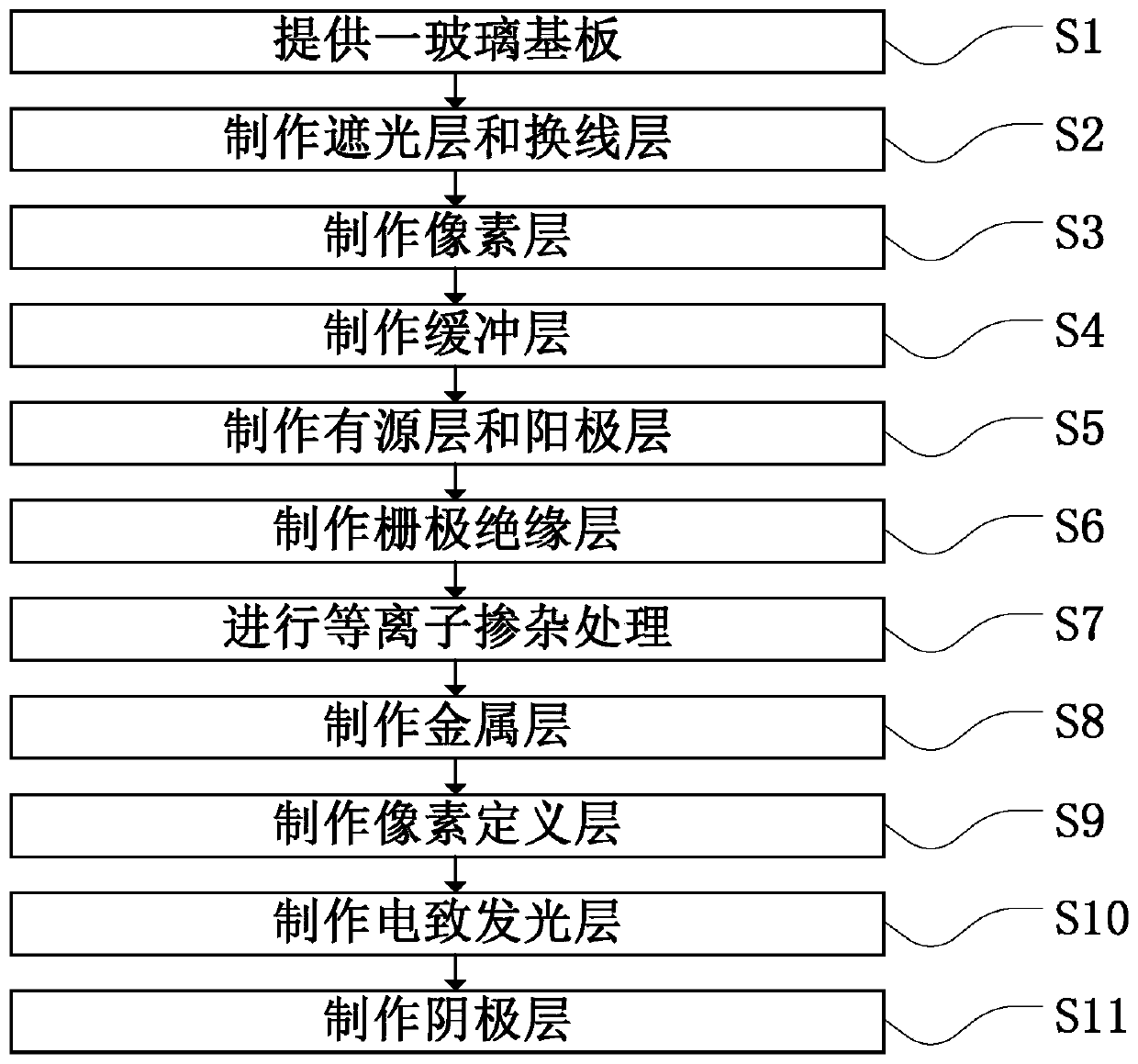
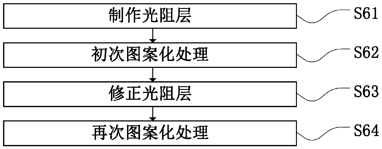
[0048] The following will clearly and completely describe the technical solutions in the embodiments of the present invention with reference to the drawings in the embodiments of the present invention. Apparently, the described embodiments are only some of the embodiments of the present invention, but not all of them. Based on the embodiments of the present invention, all other embodiments obtained by those skilled in the art without creative efforts fall within the protection scope of the present invention.

[0049] The terms "first", "second", "third", etc. (if any) in the description and claims of the present invention and the above drawings are used to distinguish similar objects and not necessarily to describe a specific order or sequentially. It should be understood that the items so described are interchangeable under appropriate circumstances. Furthermore, the terms "comprising" and "having", as well as any variations thereof, are intended to cover a non-exclusive in...


PUM


Abstract

The invention discloses an array substrate and a manufacturing method thereof. The array substrate is provided with a thin-film transistor area, a line exchange area and a light-emitting area; the thin-film transistor area comprises laminated glass substrate, light shielding layer, buffer layer, active layer, gate insulating layer, metal layer, pixel definition layer, light-emitting layer and a cathode layer; and the manufacturing method of the array substrate comprises the steps of providing the glass substrate; manufacturing the light shielding layer and the line exchange layer; manufacturing the pixel layer; manufacturing the buffer layer; manufacturing the active layer and the anode layer; manufacturing the gate insulating layer; carrying out plasma doping treatment; manufacturing themetal layer; manufacturing the pixel definition layer; manufacturing the light-emitting layer; and manufacturing the cathode layer. One mask is shared by a plurality of film layers to complete patterning when the array substrate is manufactured, thereby reducing the number of used mask, simplifying the process, improving the production efficiency, shortening the process time and reducing the cost;furthermore, the array substrate is simple and reasonable in structure; and the lightweight design is achieved.

Description

technical field [0001] The invention relates to the field of display technology, in particular to an array substrate of a top-gate thin film transistor and a manufacturing method thereof. Background technique [0002] At present, in the active matrix organic light-emitting diode (AMOLED) display device, the top-gate thin-film transistor (Top-gate TFT) array substrate has a complex structure, and the number of film layers increases the process steps. A minimum of 11 mask plates are required for the fabrication of . As we all know, each additional process step will not only increase time and material costs, but also bring the risk of process yield decline. [0003] Therefore, it is really necessary to develop a new type of array substrate and its manufacturing method to overcome the defects in the prior art. Contents of the invention [0004] The present invention provides an array substrate and a manufacturing method thereof. By changing the structure of the array substra...

Claims


Application Information

Patent Timeline
Patent Type & Authority Applications(China)
IPC IPC(8): H01L27/32H01L21/77H01L51/56
CPCH01L27/1288H10K59/12H10K59/1213H10K59/1201H10K71/00
Inventor 唐甲任章淳
Owner SHENZHEN CHINA STAR OPTOELECTRONICS SEMICON DISPLAY TECH CO LTD
Why Eureka
Try Eureka