A kind of pcb board and its manufacturing method

A technology of PCB board and board body is applied in the field of PCB board and its manufacturing to achieve the effect of increasing the heat dissipation area, preventing instantaneous temperature rise, and increasing the thermal conductivity efficiency.

Active Publication Date: 2021-02-23
WUHAN JINGLI ELECTRONICS TECH +1
View PDF3 Cites 0 Cited by
  • Summary
  • Abstract
  • Description
  • Claims
  • Application Information

AI Technical Summary

Problems solved by technology

[0005] In view of the above defects or improvement needs of the prior art, the present invention provides a PCB board and its manufacturing method, which can ensure The best PCB heat dissipation effect, and at the same time will not cause the problem of poor soldering of components

Method used


Image

  • A kind of pcb board and its manufacturing method
  • A kind of pcb board and its manufacturing method
  • A kind of pcb board and its manufacturing method

Examples


Embodiment 1

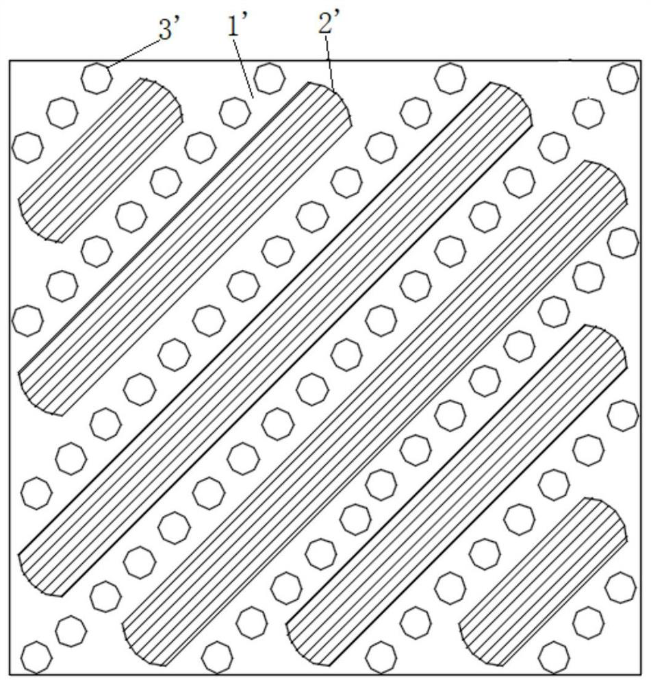
[0031] refer to figure 1 , a PCB board, including a PCB body, the PCB body has a TOP surface and a BOT surface opposite to the TOP surface, the components installed on the TOP surface are more than the BOT surface, and the BOT surface is mainly used for heat dissipation. The PCB The board body is provided with more than one via area 1', and the via area 1' is provided with a plurality of via holes 3', and the inner wall of each via hole 3' is covered with copper, wherein,

[0032] The TOP surface of the PCB body forms a first window by removing solder resist oil at the via area 1', so as to solder components after applying solder paste at the first window;

[0033] The BOT surface of the PCB body is covered with solder resist oil at the via hole area 1', and the BOT surface of the PCB body is formed by removing solder resist oil at a position adjacent to the via hole area 1' More than one second opening 2', so that the heat at the via area 1' can be conducted to the second op...

Embodiment 2

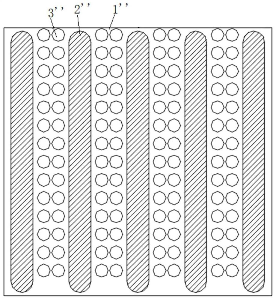
[0046] refer to figure 2 , a PCB board, including a PCB body, the PCB body has a TOP surface and a BOT surface opposite to the TOP surface, the components installed on the TOP surface are more than the BOT surface, and the BOT surface is mainly used for heat dissipation. The PCB The board body is provided with more than one via area 1", and the via area 1" is provided with a plurality of via holes 3", and the inner wall of each via hole 3" is covered with copper, wherein,

[0047] The TOP surface of the PCB body forms a first window by removing the solder resist oil at the via area 1", which is used for soldering components after applying solder paste at the first window;

[0048] The BOT surface of the PCB body is covered with solder resist oil at the via hole area 1", and the BOT surface of the PCB body is formed by removing solder resist oil at a position adjacent to the via hole area 1". More than one second opening 2", so that the heat at the via area 1" can be conducte...


PUM

PropertyMeasurementUnit
thermal conductivityaaaaaaaaaa

Abstract

The invention discloses a PCB board and a manufacturing method thereof. The PCB board includes a PCB body. The PCB body has a TOP surface and a BOT surface opposite to the TOP surface. The PCB body is provided with more than one overpass. In the hole area, each of the via area is provided with a plurality of via holes, and the TOP surface of the PCB body forms a first window by removing solder mask oil at the via area, so as to be used for soldering components ; The BOT surface of the PCB body is covered with solder resist oil at the via hole area, and the BOT surface of the PCB body forms more than one by removing the solder resist oil at a position adjacent to the via hole area Second window. The present invention staggers the second window on the BOT surface and the via hole area on the PCB body, and also covers the solder resist oil at the via hole area of ​​the BOT surface, so that tin can be avoided from passing through when soldering on the PCB board. Poor soldering of components due to hole leakage.

Description

technical field [0001] The invention belongs to the technical field of PCB board heat dissipation, and more specifically relates to a PCB board and a manufacturing method thereof. Background technique [0002] Most of the electrical energy consumed by electronic equipment during operation, such as RF power amplifiers, FPGA components, and power supply products, is converted into heat in addition to useful work. The heat generated by electronic equipment causes the internal temperature to rise rapidly. If the heat is not dissipated in time, the equipment will continue to heat up, the device will fail due to overheating, and the reliability of electronic equipment will decline. [0003] SMT (Surface Mount Technology) increases the installation density of electronic equipment, reduces the effective heat dissipation area, and the temperature rise of the equipment seriously affects the reliability. Therefore, the research on thermal design is very important. [0004] Solder past...

Claims


Application Information

Patent Timeline
Patent Type & Authority Patents(China)
IPC IPC(8): H05K1/02H05K1/11H05K1/18H05K3/34
CPCH05K1/0206H05K1/111H05K1/181H05K3/341H05K2201/09563
Inventor 张博佳
Owner WUHAN JINGLI ELECTRONICS TECH
Why Eureka
Try Eureka