

A kind of manufacturing method of laminated inductor and the manufactured device
A manufacturing method and a technology of laminated inductors, which are applied in the field of manufacturing methods and manufactured devices, can solve the problems of poor inductance quality factors and low inductance values, and achieve the effects of increasing process costs, large inductance values, and reducing occupation
- Summary
- Abstract
- Description
- Claims
- Application Information
AI Technical Summary
Problems solved by technology
Method used
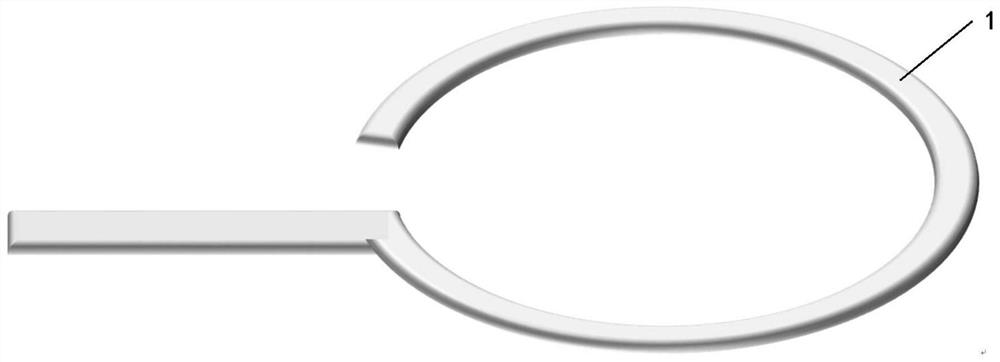
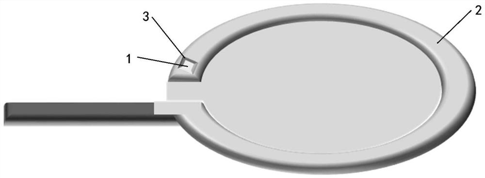
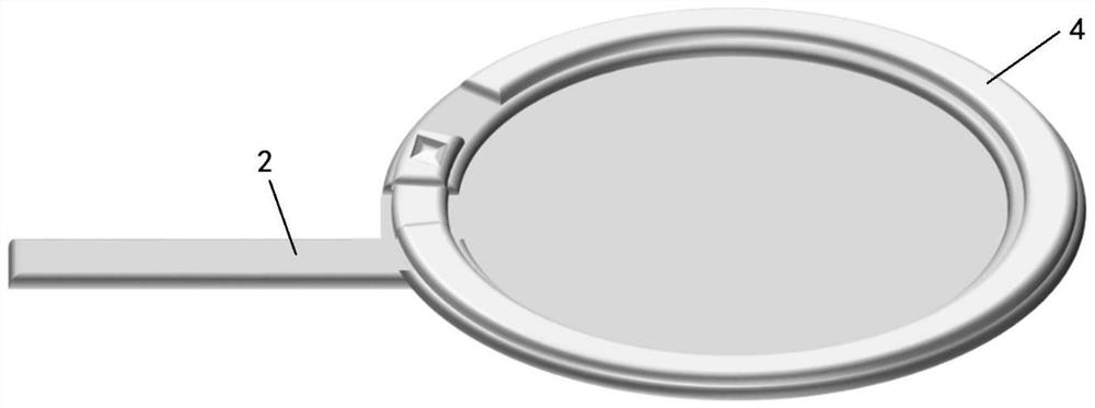
Image

Examples
Embodiment Construction
[0049] In order to explain in detail the technical content, structural features, achieved goals and effects of the technical solution, the following will be described in detail in conjunction with specific embodiments and accompanying drawings.
[0050] see Figure 1 to Figure 9 , this embodiment provides a method for manufacturing a stacked inductor. The present invention can simultaneously manufacture a transistor when making an inductor. The transistor can be a PHEMT (pseudo-modulated doped heterojunction field-effect transistor), so that the process of the inductor of the present invention The steps are performed in the same process step as the process steps of the transistor, so the process cost will not be increased. The process steps of the transistor are the process steps of the existing transistor, and the formed structure is also the existing transistor structure. The focus of the present invention is not to form the transistor structure, so the present invention doe...
PUM
 Abstract
Description
Claims
Application Information