Manufacturing method of trench type double-layer gate MOSFET

A manufacturing method and double-layer gate technology, applied in semiconductor/solid-state device manufacturing, electrical components, semiconductor devices, etc., can solve problems that affect the stability of the first contact hole, cannot guarantee complete filling, and affect product quality. Shape stability, process cost reduction, and product quality improvement

Active Publication Date: 2019-11-22
SHANGHAI HUAHONG GRACE SEMICON MFG CORP
View PDF8 Cites 4 Cited by
  • Summary
  • Abstract
  • Description
  • Claims
  • Application Information

AI Technical Summary

Problems solved by technology

[0044] Although the existing second method does not need to use a single photolithography process to protect the top of the source extraction trench before performing the etching back of the inter-polysilicon oxide layer 205; however, since the width of the source extraction trench 202b is enlarged, After the second polysilicon layer 207 is filled in step five, a gap region will be formed on the top of the source extraction trench 202b, and the gap region will increase after the second polysilicon layer 207 is etched back, which will make the growth in step seven After the metal lower dielectric layer 208, it cannot be guaranteed that the metal lower dielectric layer 208 will completely fill the gap area at the top of the source extraction trench 202b, which will affect the stability of the subsequent first contact hole, thereby affecting the quality of the product

Method used


Image

  • Manufacturing method of trench type double-layer gate MOSFET
  • Manufacturing method of trench type double-layer gate MOSFET
  • Manufacturing method of trench type double-layer gate MOSFET

Examples


Embodiment Construction

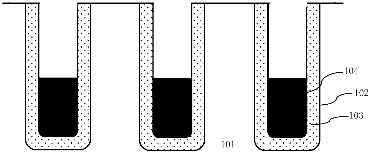
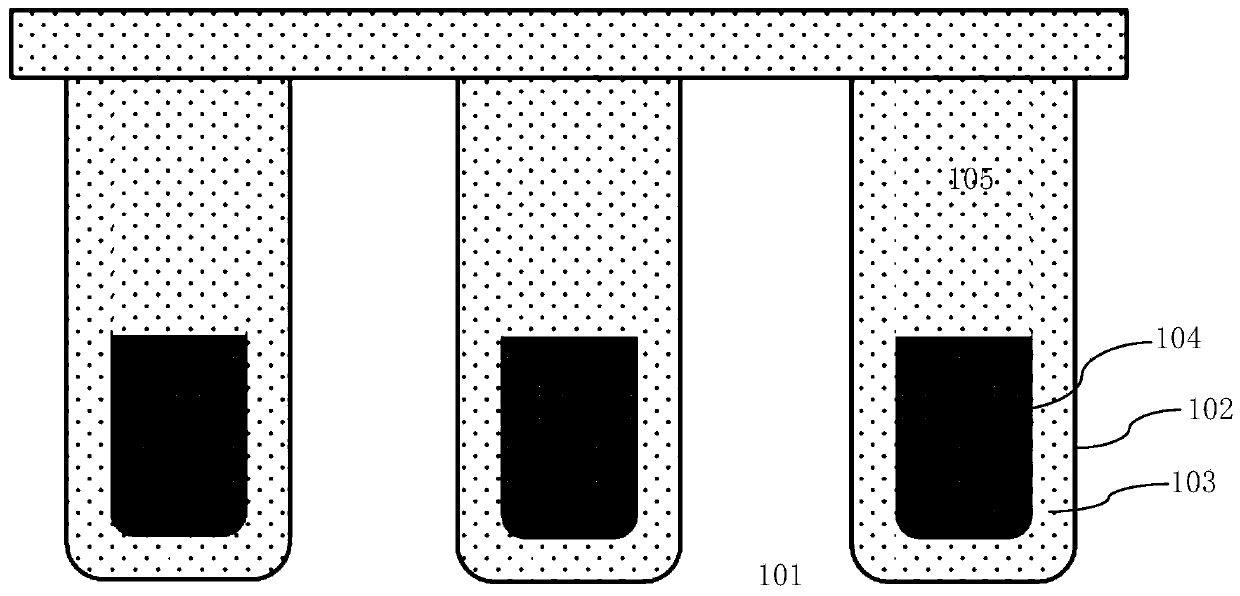
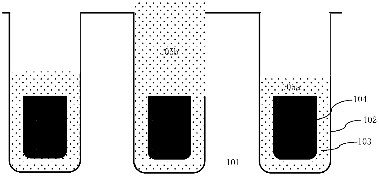
[0080] Such as image 3 As shown, it is a flow chart of the manufacturing method of the trench type double-layer gate MOSFET according to the embodiment of the present invention; as shown in Fig. 4A to Figure 4H Shown is a schematic diagram of the device structure in each step of the method of the embodiment of the present invention; the manufacturing method of the trench type double-layer gate MOSFET of the embodiment of the present invention includes the following steps:

[0081] Step 1, such as Figure 4A As shown, a plurality of trenches are formed on the semiconductor substrate 1 by photolithography definition plus etching process, the trenches include a plurality of gate trenches 2a and at least one source extraction trench 2b, and the gate trenches 2a are formed In the device unit area, the source extraction trench 2b is located outside the device unit area, the source extraction trench 2b communicates with each of the gate trenches 2a, and the source extraction trenc...


PUM


Abstract

The invention discloses a manufacturing method of a trench type double-layer gate MOSFET, which comprises the following steps of: forming a plurality of trenches which comprise a plurality of gate trenches and at least one source lead-out trench; forming a bottom dielectric layer and source polysilicon; forming an inter-polycrystalline silicon oxide layer by adopting an HDP CVD deposition and backetching process; forming a gate dielectric layer; performing polycrystalline silicon deposition to form a second polycrystalline silicon layer; etching back the second polycrystalline silicon layer,forming a polycrystalline silicon gate by the second polycrystalline silicon layer filled in the gate trench after etching back, and reserving the remaining second polycrystalline silicon layer on theside surface of the source lead-out trench; carrying out growth of an under-metal dielectric layer, wherein the growth thickness being greater than a target thickness, and the growth thickness of theunder-metal dielectric layer satisfying complete filling of a gap region in the source lead-out trench; carrying out wet etching to reduce the thickness of the metal lower dielectric layer to a target thickness; performing etching to form an opening of the contact hole, and filling metal. The process cost can be reduced, and the product quality can be improved.

Description

technical field [0001] The invention relates to a method for manufacturing a semiconductor integrated circuit, in particular to a method for manufacturing a trench type double-layer gate MOSFET. Background technique [0002] The existing first manufacturing method of trench double-layer gate MOSFET: [0003] Such as Figure 1A to Figure 1F Shown is a schematic diagram of the device structure in each step of the existing first trench type double-layer gate MOSFET manufacturing method; the existing first trench type double-layer gate MOSFET manufacturing method includes the following steps: [0004] Step 1, such as Figure 1A As shown, a plurality of trenches 102 are formed on a semiconductor substrate 101 by photolithography definition plus etching process, and the trenches 102 include a plurality of gate trenches and at least one source extraction trench, and the gate trenches are formed in In the device unit area, the source extraction trench is located outside the device...

Claims


Application Information

Patent Timeline
IPC IPC(8): H01L21/28H01L21/768
CPCH01L21/76897H01L29/401
Inventor 顾昊元蔡晨
Owner SHANGHAI HUAHONG GRACE SEMICON MFG CORP
Why Eureka
Try Eureka