Doping method, single crystal device and single crystal furnace

A single crystal furnace and single crystal technology, applied in the direction of single crystal growth, single crystal growth, chemical instruments and methods, etc., can solve the problems that the resistance uniformity of single crystal silicon rods cannot meet the standard and affect the quality of single crystal silicon rods, etc.

Inactive Publication Date: 2019-12-03
NINGXIA LONGI SILICON MATERIALS
View PDF8 Cites 1 Cited by
  • Summary
  • Abstract
  • Description
  • Claims
  • Application Information

AI Technical Summary

Problems solved by technology

[0004] The invention provides a doping method, a single crystal device and a single crystal furnace, aiming to solve the problem that the resistance uniformi

Method used


Image

  • Doping method, single crystal device and single crystal furnace
  • Doping method, single crystal device and single crystal furnace
  • Doping method, single crystal device and single crystal furnace

Examples


Embodiment 1

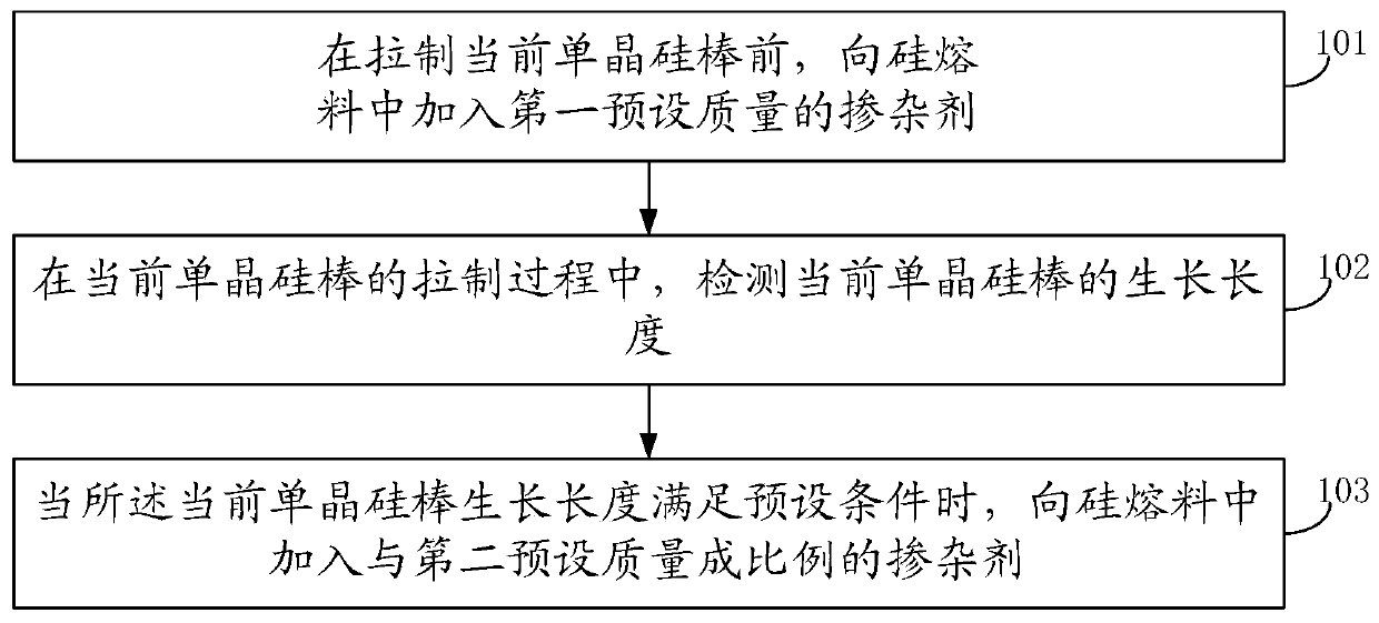
[0046] refer to figure 1 , figure 1 It shows a flow chart of the steps of a doping method according to Embodiment 1 of the present invention, the method comprising:

[0047] Step 101 , before pulling the current single crystal silicon rod, adding a first preset mass of dopant to the silicon melt.

[0048] In the embodiment of the present invention, before pulling the current single crystal silicon rod, a dopant of a first preset quality is added to the silicon melt, and adding the dopant of the first preset quality to the silicon melt is In order to ensure that the initially generated part of the current single crystal silicon rod is doped with dopants when the current single crystal silicon rod is drawn, and because the crucible rotates when the current single crystal silicon rod is drawn, a centripetal force is generated, so that the doped The dopant is evenly distributed on the surface of the silicon melt, so that the dopant distribution in the current monocrystalline sil...

Embodiment 2

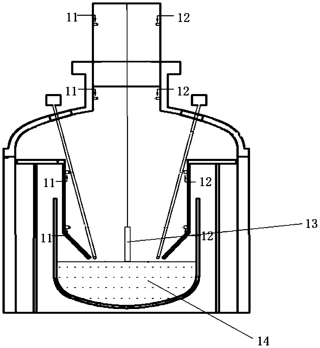
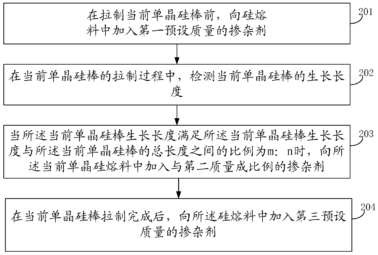
[0063] refer to image 3 , image 3 It shows a flow chart of steps of a doping method in Embodiment 2 of the present invention, the method includes: the method is applied to Figure 4 shown in the single crystal furnace, refer to Figure 4 , the single crystal furnace includes a dopant 10, a photosensitive sensor and a controller (not shown in the figure); the dopant 10 is arranged in the single crystal furnace through an opening 15 on the single crystal furnace, and the photosensitive sensor It includes a photosensitive sensor transmitting end 11 and a photosensitive sensor receiving end 12 . The photosensitive sensor is connected with the controller, and the controller is connected with the dopant 10 . Step 201, before pulling the current single crystal silicon rod, adding a dopant of a first preset quality into the silicon melt.

[0064] In the embodiment of the present invention, the steps are the same as step 101 in the first embodiment, and will not be repeated here....

Embodiment 3

[0095] refer to Figure 5 , shows that the embodiment of the present invention discloses a single crystal device 30, and the single crystal device 30 includes: a first control module 301, a detection module 302 and a second control module 303;

[0096] The first control module 301 is used to add a dopant of a first preset quality to the silicon melt before pulling the current single crystal silicon rod;

[0097] The detection module 302 is used to detect the growth length of the current single crystal silicon rod during the current pulling process of the single crystal silicon rod;

[0098] The second control module 303 is configured to add a dopant proportional to a second preset mass to the molten silicon when the growth length of the current single crystal silicon rod satisfies a preset condition.

[0099] Optionally, the preset condition includes: the ratio between the growth length of the current single crystal silicon rod and the preset total length of the current singl...


PUM


Abstract

The invention provides a doping method, a single crystal device and a single crystal furnace. The method comprises the following steps: adding a dopant with a first preset mass into a silicon melt before a current monocrystalline silicon rod is drawn; detecting the growth length of the current monocrystalline silicon rod in a drawing process of the current monocrystalline silicon rod; and adding adopant proportional to a second preset mass into the silicon melt when the growth length of the current monocrystalline silicon rod meets a preset condition. According to the invention, addition of the dopant and drawing of the current monocrystalline silicon rod can be carried out synchronously; in the drawing process of the monocrystalline silicon, the dopant is added into the silicon melt whenthe growth length of the current monocrystalline silicon rod meets the preset condition; and due to centripetal force generated by rotation of a crucible, the dopant can be uniformly distributed on the surface of the silicon melt, so that uniformity of the dopant in each part of a drawn current monocrystalline silicon rod is ensured, resistance uniformity of the prepared current monocrystalline silicon rod is improved, and then the actual yield of the current monocrystalline silicon rod is improved.

Description

technical field [0001] The invention relates to the technical field of manufacturing single crystal silicon rods, in particular to a doping method, a single crystal device and a single crystal furnace. Background technique [0002] In the process of preparing solar-grade or semiconductor-grade single crystal silicon rods, dopants are usually added to the silicon melt in the crucible of the single crystal furnace, and then pulled through the single crystal furnace to form single crystal silicon rods. [0003] Due to the unstable operation of the production line in the current preparation process of single crystal silicon rods, and the difference in the concentration of dopants in the silicon melt of each layer in the crucible, the resistance uniformity of the prepared single crystal silicon rods is difficult to meet Standards, which in turn affect the quality of monocrystalline silicon rods. Contents of the invention [0004] The invention provides a doping method, a singl...

Claims


Application Information

Patent Timeline
IPC IPC(8): C30B15/04C30B15/20C30B29/06
CPCC30B15/04C30B15/20C30B29/06
Inventor 锁志云李强涂准
Owner NINGXIA LONGI SILICON MATERIALS
Why Eureka
Try Eureka