FPGA (Field Programmable Gate Array) switch unit based on STT-MRAM (Short Term Transistor-Magnetic Random Access Memory)

A switching unit and control unit technology, applied in the field of integrated circuits, can solve the problems of high cost of FLASH type FPGA, poor reliability of SRAM type FPGA, loss of data after power failure, etc. effect of times

Active Publication Date: 2019-12-03
58TH RES INST OF CETC
View PDF4 Cites 5 Cited by
  • Summary
  • Abstract
  • Description
  • Claims
  • Application Information

AI Technical Summary

Problems solved by technology

[0004] The object of the present invention is to provide a kind of FPGA switch unit based on STT-MRAM, to solve traditional SRAM type FPGA poor reliability, power-off data loss, and the problem of high cost and low operating frequency of FLASH type FPGA

Method used


Image

  • FPGA (Field Programmable Gate Array) switch unit based on STT-MRAM (Short Term Transistor-Magnetic Random Access Memory)
  • FPGA (Field Programmable Gate Array) switch unit based on STT-MRAM (Short Term Transistor-Magnetic Random Access Memory)
  • FPGA (Field Programmable Gate Array) switch unit based on STT-MRAM (Short Term Transistor-Magnetic Random Access Memory)

Examples


Embodiment 1

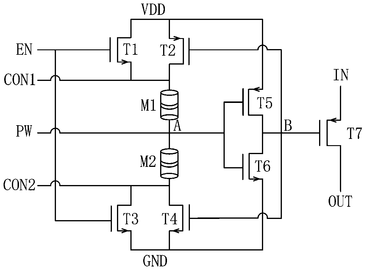
[0030] The present invention provides a FPGA switch unit based on STT-MRAM, comprising an STT-MRAM element group, a control unit, an inverter and a switch unit; wherein, the STT-MRAM element group generates a potential to the inverter, The inverter inverts the potential and feeds it back to the control unit, and the control unit controls the potential latch of the STT-MRAM element group under the action of the inverter; the switch unit is connected to the connected to the output of the inverter. Through the feedback effect of the inverter, the FPGA switch unit is in the working mode, and the two ends of the STT-MRAM element group are always in an equipotential state, reducing the electrical stress effect on the STT-MRAM element in the STT-MRAM element group , improve the reliability of the device.

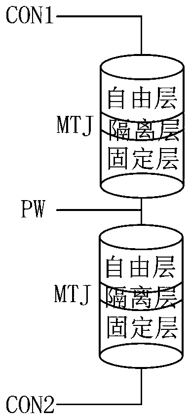
[0031] Specifically, an implementation structure of the FPGA switch unit based on STT-MRAM is as follows figure 1 shown. The STT-MRAM element group includes several STT-MRAM ele...

Embodiment 2

[0045] Embodiment 2 of the present invention provides another implementation of the FPGA switch unit based on STT-MRAM, such as Figure 4 shown. Compared with the first embodiment, the control unit includes PMOS transistors T1, T2, T3 and NMOS transistor T4; wherein, the gate of the PMOS transistor T1 is connected to the control signal EN, the source is connected to the power supply VDD, and the drain is connected to the PMOS transistor T2. Drain: the gate of the PMOS transistor T2 is connected to the output terminal of the inverter, the source is connected to the power supply VDD, and the drain is connected to the STT-MRAM element group, that is, the free layer of the STT-MRAM element M1; the PMOS transistor The gate of T3 is connected to the control signal EN, the drain is grounded to GND, the source is connected to the drain of the NMOS transistor T4; the gate of the NMOS transistor T4 is connected to the output terminal of the inverter, the source is grounded to GND, and t...


PUM


Abstract

The invention discloses an FPGA switch unit based on an STT-MRAM, and belongs to the technical field of integrated circuits. The FPGA switch unit based on the STT-MRAM comprises an STT-MRAM element group, a control unit, a phase inverter and a switch unit. The STT-MRAM element group generates an electric potential to the phase inverter. The phase inverter inverts the electric potential and feeds back the electric potential to the control unit. The control unit controls the electric potential latch of the STT-MRAM element group under the action of the phase inverter; and the switch unit is connected with the output end of the phase inverter. The FPGA switch unit can realize that data configured in the STT-MRAM element group cannot be lost after the FPGA is powered down. Compared with a traditional SRAM type FPGA, the FPGA does not need to read data from an external independent memory for operation when powered on, and the starting speed is high. Due to the fact that the STT-MRAM elementset is high in read-write speed and low in power consumption, compared with a FLASH type FPGA, the FPGA switch unit has the higher read-write frequency, the higher erasing and writing frequency and the lower cost.

Description

technical field [0001] The invention relates to the technical field of integrated circuits, in particular to an FPGA switch unit based on STT-MRAM. Background technique [0002] FPGA (Field-Programmable Gate Array) is a semi-customized field-programmable logic gate array. Due to its short development cycle, high cost performance, and good flexibility, it is widely used in communications, aerospace, automotive, medical, and process control. and other fields. [0003] There are currently three main types of FPGA technology: FPGA technology configured with SRAM, FPGA technology configured with antifuse, and FPGA technology configured with Flash. Among them, the SRAM-configured FPGA has the advantages of fast speed, unlimited programming times, and strong process compatibility, and is currently the mainstream FPGA configuration technology; the anti-fuse-configured FPGA has the characteristics of non-volatility compared with the SRAM-configured FPGA. It can solve the problem of...

Claims


Application Information

Patent Timeline
Patent Type & Authority Applications(China)
IPC IPC(8): G06F15/78
CPCG06F15/7867Y02D10/00
Inventor 张海良施辉曹利超宋思德吴建伟洪根深
Owner 58TH RES INST OF CETC
Why Eureka
Try Eureka