Laser direct writing micro-nano structure system based on single-wavelength double beams and method

A technology of laser direct writing and micro-nano structure, applied in the field of laser direct writing micro-nano structure system, can solve the problems of different spot sizes, weakening the integration degree of processing system, and restricting system expansion and integration.

Active Publication Date: 2019-12-10
JINAN UNIVERSITY
View PDF6 Cites 9 Cited by
  • Summary
  • Abstract
  • Description
  • Claims
  • Application Information

AI Technical Summary

Problems solved by technology

On the premise that the material properties meet the aforementioned two-photon absorption and the subsequent photochemical process can be effectively suppressed, there may be problems in optical design: First, two beams of light of different colors require at least two kinds of lasers, which increases the processing cost and weakens the Processing system development can be integrated; secondly, after the two beams of different colors are focused by the lens, due to the different wavelengths, the size of the focused spot is different, and there are certain difficulties and deviations in judging the spatial overlap. The degree of inferiority is the key to the final result; again, in the design of the optical path after the spatial combination of two laser beams of different colors, the optical element needs to satisfy the photoresponse characteristics of the two different colors at the same time, and support the near-infrared and visible light bands at the same time. It is bound to introduce the problems of dispersion and low energy utilization, and bring about the complexity of the system and increase the cost of optical design; finally, the complexity of wavelength matching of optical components will limit the further expansion and integration of the system, which is not conducive to the entire processing Systematization and integration of methods

Method used


Image

  • Laser direct writing micro-nano structure system based on single-wavelength double beams and method
  • Laser direct writing micro-nano structure system based on single-wavelength double beams and method
  • Laser direct writing micro-nano structure system based on single-wavelength double beams and method

Examples


Embodiment Construction

[0036] The present invention will be further described below in conjunction with drawings and embodiments.

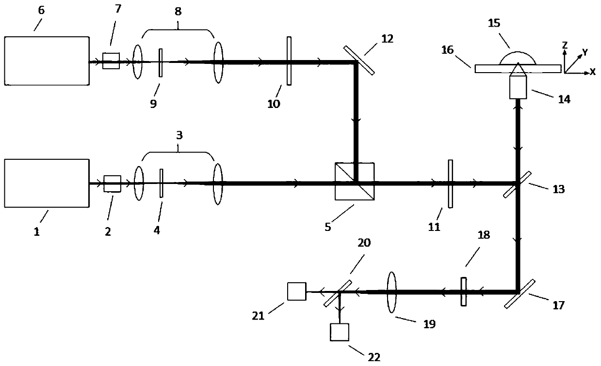
[0037] see figure 1 , one A laser direct writing micro-nano structure system based on single-wavelength and double-beams, comprising: a pulsed laser 1, a first high-speed optical switch 2, a first 4f lens group 3, a first spatial filter aperture 4, a polarizing beam splitter 5, CW laser 6, second high-speed optical switch 7, second 4f lens group 8, second spatial filter aperture 9, spiral phase plate 10, quarter slide 11, first mirror 12, first semi-anti-half Lens 13, objective lens 14, sample to be photoetched 15, displacement platform 16, second mirror 17, optical filter 18, convex lens 19, second half mirror 20, charge-coupled device image sensor 21 and avalanche photodiode 22 The pulse laser 1, the first high-speed optical switch 2 and the first 4f lens group 3 are arranged in sequence, and the first spatial filter aperture 4 is arranged between different lenses ...


PUM

PropertyMeasurementUnit
wavelengthaaaaaaaaaa

Abstract

The invention discloses a laser direct writing micro-nano structure system based on single-wavelength double beams. The system comprises a pulse laser device 1, a first high-speed optical switch 2, afirst 4f lens group 3, a first spatial filtering small hole 4, a polarization beam splitter 5, a continuous laser device 6, a second high-speed optical switch 7, a second 4f lens group 8, a second spatial filtering small hole 9, a spiral phase plate 10, a quarter-wave slide 11, a first reflector 12, a first semi-reflective semi-transparent mirror 13, an objective lens 14 and a to-be-photoetched sample 15. The system is advantaged in that two beams of laser with the same wavelength are selected as an excitation light source and a suppression light source respectively, high transient light intensity of the exciting light is utilized to ensure that nonlinear absorption of the material is used for initiating photopolymerization reaction, micro-nano structure processing is realized, the phase modulation technology is combined to adjust an inhibiting light focus into a hollow shape, so polymerization reaction is further localized in the central area of the exciting light, and a purpose of compressing the polymerization size is achieved.

Description

technical field [0001] The invention relates to the technical field of nano-processing, in particular to a system and method for laser direct writing of micro-nano structures based on single-wavelength and double-beams. Background technique [0002] Femtosecond laser direct writing technology has been widely used in many industrial manufacturing and scientific research fields due to its advantages of high processing precision, small thermal effect, low damage threshold, and the ability to process any three-dimensional graphics. The traditional single-beam femtosecond laser direct writing processing method, with the help of the nonlinear two-photon absorption process of the processing material, combined with the threshold effect of the material, can use visible light to achieve micron and sub-micron scale processing accuracy, but the processing resolution is still affected by optical diffraction. The limit limit restricts its further development. [0003] In order to solve t...

Claims


Application Information

Patent Timeline
Patent Type & Authority Applications(China)
IPC IPC(8): G03F7/20G02B27/09G02B27/28
CPCG02B27/0927G02B27/0955G02B27/0977G02B27/283G03F7/70383G03F7/7055
Inventor 曹耀宇谢飞
Owner JINAN UNIVERSITY
Why Eureka
Try Eureka