Clock generator circuit and clock generation method
A clock generation circuit and clock generator technology, applied to electrical components, amplifiers with semiconductor devices/discharge tubes, automatic power control, etc., can solve problems that affect loop performance, loop instability, and failure to operate
- Summary
- Abstract
- Description
- Claims
- Application Information
AI Technical Summary
Problems solved by technology
Method used
Image


Examples
no. 1 example
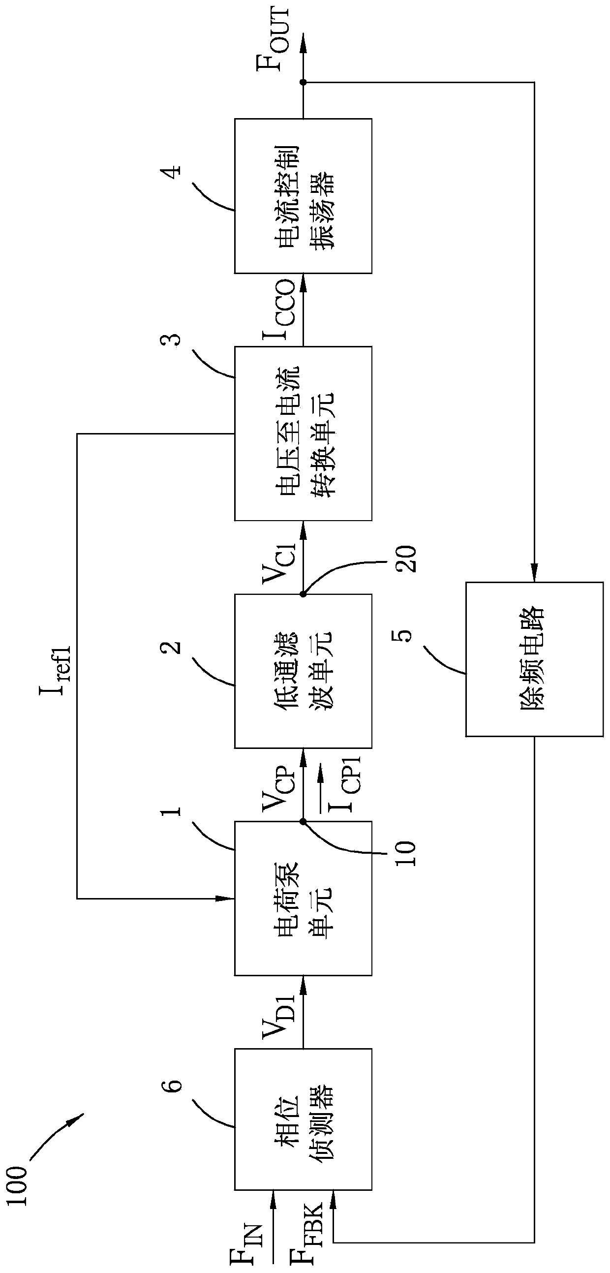
[0036] see figure 1 , is the first embodiment of the clock generating circuit 100 of the present invention, including a charge pump (ChargePump; CP) unit 1, a low-pass filter (Low-Pass Filter; LPF) unit 2, a voltage-to-current conversion unit (V-I Converter) 3, and a current-controlled clock generator. Here, the current-controlled clock generator is illustrated by taking a current-controlled oscillator (Current Controlled Oscillator; CCO) 4 as an example, wherein the charge pump unit 1 can be coupled to a phase detector Detector (Phase Detector; PD) 6, and the current-controlled oscillator 4 can be coupled to a frequency divider circuit (Frequency Divider) 5, thereby forming a phase-locked loop (PLL).
[0037] The frequency dividing circuit 5 receives an output clock signal F OUT , and generate a frequency-divided clock signal F FBK , and the output clock signal F OUT The frequency is divided by the frequency-divided clock signal F FBK The frequency of is equal to a predet...
no. 2 example
[0054] see figure 1 and image 3 , is the second embodiment of the present invention, derived from the first embodiment, wherein the voltage-to-current conversion unit 3 includes a first voltage-to-current converter 32, which includes a first operational amplifier (Operational Amplifier; OP) 321 and a second resistive element K VI1 .
[0055] The first operational amplifier 321 includes a positive input terminal, a negative input terminal, and an output terminal coupled to the negative input terminal, and is also coupled to the first charge pump 11 of the charge pump unit 1 . The first operational amplifier 321 is used as a single-gain buffer, and is coupled to the first filter 21 of the low-pass filter unit 2 through the positive input terminal to receive the first control voltage V C1 , and through its output coupled to the second resistive element K VI1 to generate the control current I CCO , and generate the first reference current I for the charge pump unit 1 to receiv...
no. 3 example
[0060] see figure 1 and Figure 5 , Figure 5 It is the third embodiment of the present invention, which is derived from the second embodiment. In this embodiment, the first filter 21 of the low-pass filter unit 2 and the first filter 21 of the voltage-to-current conversion unit 3 The voltage-to-current converter 33 shares the same operational amplifier, that is, the first operational amplifier 331 , and its design is the same as that of the first operational amplifier 321 in the second embodiment. Although the present embodiment discloses sharing the same operational amplifier, the first filter 21 and the first voltage-to-current converter 33 can also use different operational amplifiers respectively, and its design method is the same as that of the first operational amplifier of the present embodiment. Amplifier 321 is the same.
[0061] The first operational amplifier 331 includes a positive input terminal receiving a reference voltage and a positive input terminal coupl...
PUM
 Abstract
Description
Claims
Application Information