

Image sensor device and manufacturing method thereof
A technology for image sensors and sensor chips, applied in radiation control devices, electric solid devices, semiconductor devices, etc., can solve the problems of reduced yield and unfavorable yield, and achieve the effects of preventing peeling, improving production efficiency, and avoiding stress problems
- Summary
- Abstract
- Description
- Claims
- Application Information
AI Technical Summary
Problems solved by technology
Method used
Image

Examples
no. 1 example
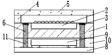
[0062] see figure 1 , the image sensor device of this embodiment is obtained by bonding a first bonding portion and a second bonding portion, wherein, the first bonding portion, the first bonding portion includes a semiconductor substrate 1, a spacer 4 and cover glass5. The semiconductor substrate 1 is a traditional silicon material, which is cut from a semiconductor wafer, and has pads 3 and sensor chip regions 2 on its upper surface, and the pads 3 are connected to the sensor chip region 2 .
[0063] The cover glass 5 is adhered on the upper surface of the semiconductor substrate 1 through the spacer 4 . Wherein, the cover glass can be a glass plate with a filter layer; the semiconductor substrate 1 is provided with a first through hole 6, and the lower surface of the semiconductor substrate 1 and the lower surface of the first through hole 6 The surfaces are coplanar and constitute a first bonding plane.
[0064] The manufacturing method of the first bonding part can be ...
no. 2 example
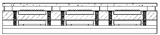
[0069] see Figure 4 , the image sensor device of this embodiment is obtained by bonding the first bonding part and the second bonding part, and its structure is basically similar to that of the first embodiment (the same reference numerals are omitted). Corresponding to the first bond, however, this exemplary embodiment additionally has a polymer layer 12 on the underside of the semiconductor substrate 1 into which the first via 6 extends. 12, the lower surface of the polymer layer 12 is coplanar with the lower surface of the first through hole 6 and constitutes a first bonding surface. The polymer layer 12 is made of the same material as the encapsulation resin layer 10 , such as epoxy resin, silicone resin, etc., so as to ensure the reliability of bonding and prevent peeling.
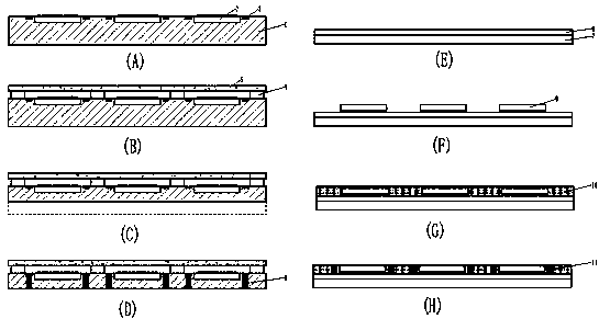
[0070] For the manufacturing method of the first bonding part of this embodiment, please refer to Figure 5 , which includes: (1) see Figure 5 (A), providing a semiconductor substrate 1 with a pl...
no. 3 example
[0074] see Figure 7 , the image sensor device of this embodiment is obtained by bonding the first bonding part and the second bonding part, and its structure is basically similar to that of the first embodiment (the same reference numerals are omitted). But corresponding to the second bond, this embodiment additionally has a redistribution layer 13 on the upper surface of the encapsulation resin layer 10, the topmost layer of the redistribution layer 13 includes a dielectric layer 14 and embedding the dielectric layer 14 The bump 15, wherein the upper surface of the dielectric layer 14 is coplanar with the upper surface of the bump 15 and constitutes a second bonding surface. The dielectric layer 14 is an inorganic insulating layer, such as silicon oxide or silicon nitride, which can ensure the reliability of the bonding between the dielectric layer 14 and the semiconductor substrate 1 (such as a silicon substrate) and prevent peeling.
[0075] For the manufacturing method o...
PUM
 Abstract
Description
Claims
Application Information