Optical measurement method for resistivity of semiconductor material

An optical measurement and semiconductor technology, used in measurement devices, analysis materials, measurement of electrical variables, etc., can solve the problems of increasing measurement errors, large probe sampling volume, material surface damage, etc., to improve measurement accuracy and small volume. Effect

Active Publication Date: 2020-01-03
XIAN TECHNOLOGICAL UNIV
View PDF6 Cites 2 Cited by
  • Summary
  • Abstract
  • Description
  • Claims
  • Application Information

AI Technical Summary

Problems solved by technology

[0003] The invention provides an optical measurement method for the resistivity of semiconductor materials in order to solve the problems of damage to the surface of the material, increase of measurement error and large probe sampling volume existing in the existing semiconductor material resistivity measurement technology

Method used


Image

  • Optical measurement method for resistivity of semiconductor material
  • Optical measurement method for resistivity of semiconductor material
  • Optical measurement method for resistivity of semiconductor material

Examples


Embodiment Construction

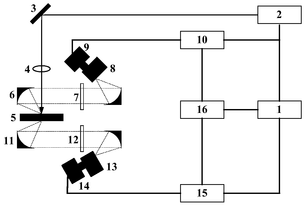
[0023] In order to make the object, technical solution and advantages of the present invention clearer, the present invention will be further described in detail below in conjunction with the accompanying drawings and embodiments. It should be understood that the specific embodiments described here are only used to explain the present invention, not to limit the present invention.

[0024] Principle of the present invention is:

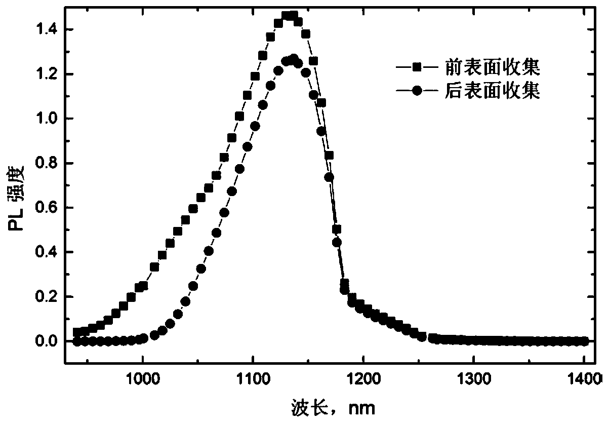
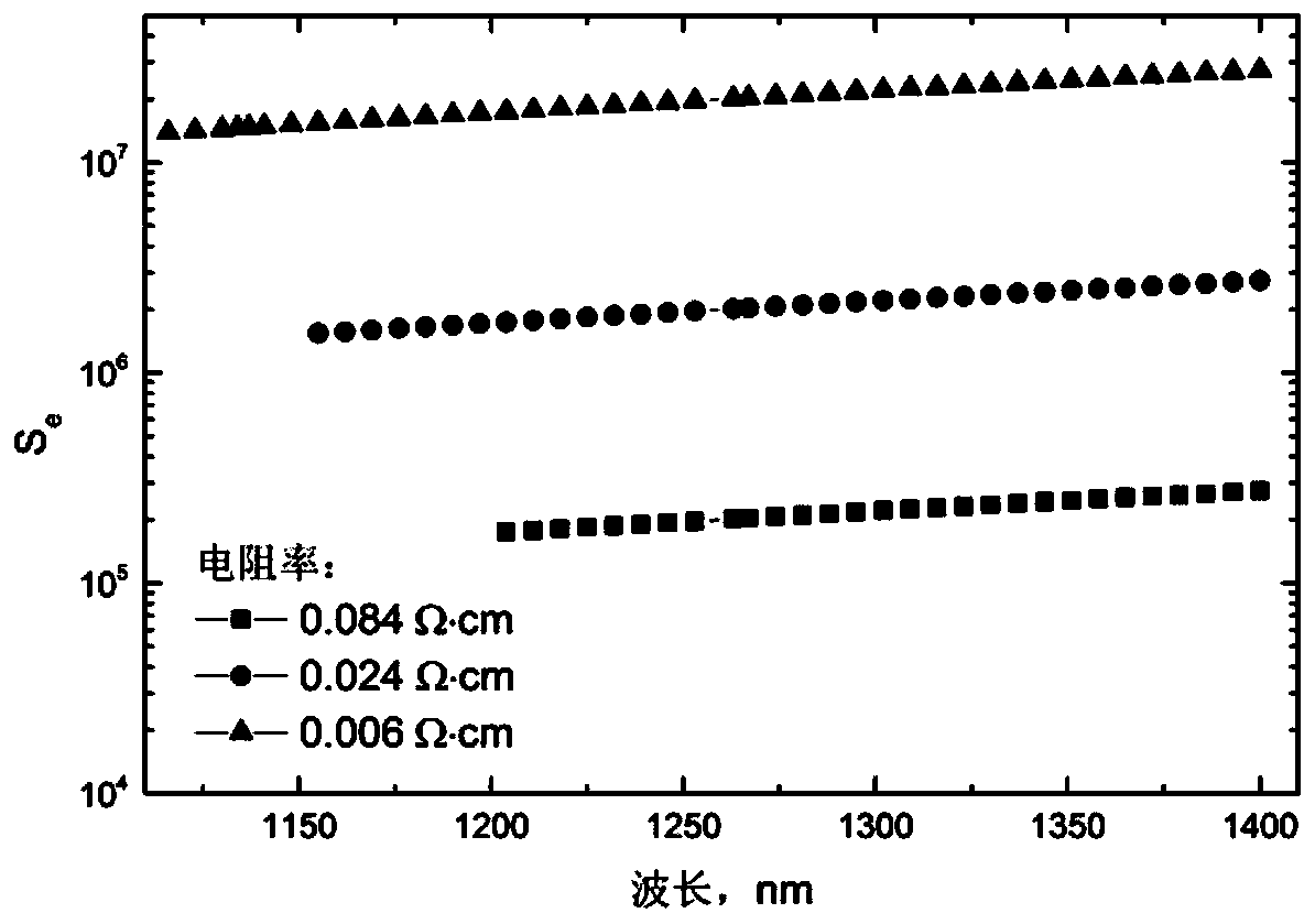
[0025] The semiconductor material absorbs the pump beam with photon energy greater than its forbidden band width to generate excess carriers, and the excess carriers generate photons after radiation recombination, and the photons are reabsorbed by the material during the transmission to the front and back surfaces. The size of the coefficient is related to the photon energy, plus the difference in the photon transmission path, the front and rear surfaces are collected and measured with different photoluminescence spectra. The reabsorption of photons ...


PUM

PropertyMeasurementUnit
reflectanceaaaaaaaaaa

Abstract

The invention relates to an optical measurement method for resistivity of a semiconductor material. The principle of the optical measurement method is as follows: a semiconductor material generates excess carriers after absorption of a pump beam with the photon energy greater than the forbidden bandwidth; the excess carriers are subjected to radiative recombination to generate photons, and the photons are reabsorbed by the material during the process of transmitting the photons to the front and back surfaces; since the magnitude of a re-absorption coefficient is related to the photon energy, in addition to the difference in photon transmission paths, the photoluminescence spectra collected and measured by the front and back surfaces are different. The re-absorption of the photons mainly comprises intrinsic absorption and free carrier absorption; the magnitude of the free carrier absorption is related to the doping concentration of the semiconductor material, therefore, the doping concentration of the semiconductor material can be obtained by analyzing and calculating the photoluminescence spectra collected by the front and back surfaces, and the resistivity can be further calculated by a formula. According to the method of the invention, the defect that a traditional four point probe technology needs to be in contact with a sample is overcome, and the measurement precision of the resistivity of the semiconductor material is improved.

Description

technical field [0001] The invention relates to an optical measurement method for resistivity of semiconductor materials. Background technique [0002] The resistivity of semiconductor materials is closely related to parameters such as series resistance, capacitance and threshold voltage of semiconductor devices, and is a very important parameter. In order to ensure that semiconductor materials can be effectively used in devices and improve device stability and yield, it is necessary to perform accurate and rapid non-destructive measurement and characterization. At present, the most commonly used resistivity measurement method for semiconductor materials in the industry is the four-probe technique. However, since this technique needs to be in contact with the sample to be tested during the measurement process, it will inevitably cause damage to the material surface and increase the measurement error. At the same time, due to the large sampling volume of the probe, its appl...

Claims


Application Information

Patent Timeline
Patent Type & Authority Applications(China)
IPC IPC(8): G01N21/63G01R27/02
CPCG01N21/636G01R27/02
Inventor 王谦刘卫国谭林秋
Owner XIAN TECHNOLOGICAL UNIV
Why Eureka
Try Eureka