
On-chip integrated graphene silicon dioxide optical waveguide saturable absorber and preparation method thereof

A silicon dioxide, optical waveguide technology, applied in lasers, laser parts, electrical components and other directions, can solve the problems of large size, reduced laser cavity length, disadvantages, etc., to improve the saturable absorption extinction ratio, improve system stability, Enhance the effect of interaction force

Inactive Publication Date: 2020-01-03
WUHAN POST & TELECOMM RES INST CO LTD +1
View PDF12 Cites 0 Cited by
  • Summary
  • Abstract
  • Description
  • Claims
  • Application Information

AI Technical Summary

Problems solved by technology

The evanescent field of this type of structured optical waveguide and the contact area of ​​graphene are small, resulting in insufficient interaction between graphene and the light field, and a low saturated absorption extinction ratio, which is not conducive to reducing the femtosecond pulse width.
In addition, the size of the optical device is relatively large, generally at the centimeter level, which is not conducive to reducing the cavity length of the laser, resulting in a low repetition rate of the laser

Method used


Image

  • On-chip integrated graphene silicon dioxide optical waveguide saturable absorber and preparation method thereof
  • On-chip integrated graphene silicon dioxide optical waveguide saturable absorber and preparation method thereof
  • On-chip integrated graphene silicon dioxide optical waveguide saturable absorber and preparation method thereof

Examples


Embodiment Construction

[0034] The present invention will be described in further detail below in conjunction with the accompanying drawings and embodiments.

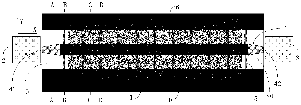
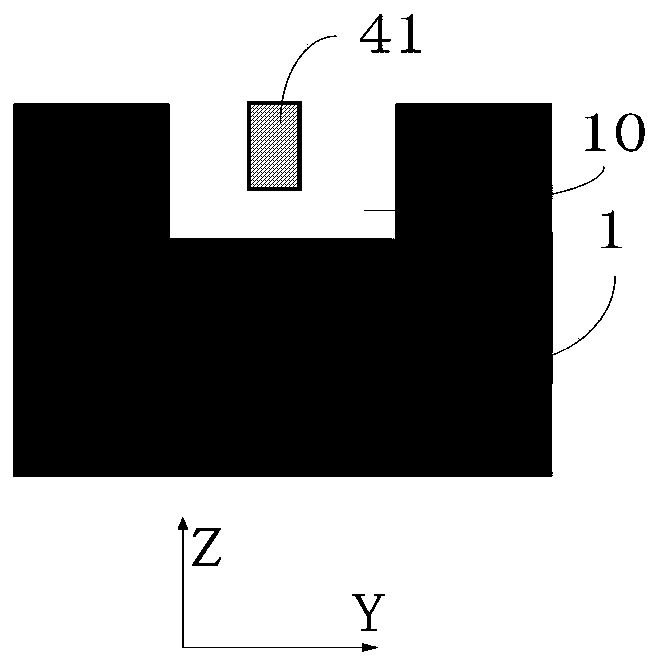
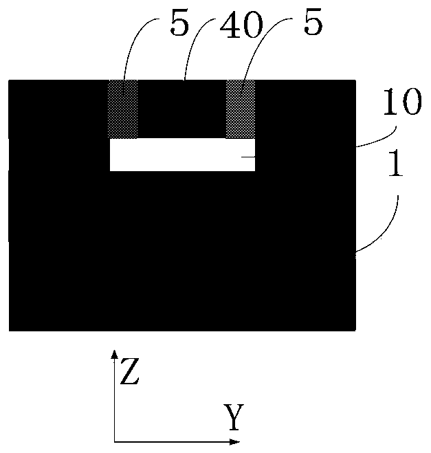
[0035] see figure 1 , and combine Figure 2 to Figure 6 For understanding, the embodiment of the present invention provides an on-chip integrated graphene silicon dioxide optical waveguide saturable absorber, which includes a substrate 1, a silicon dioxide optical waveguide 4 and a graphene film 6; the length, width and The height directions are respectively defined as X, Y, and Z directions, and a receiving groove 10 is opened on the upper surface of the substrate 1, figure 1 The accommodating groove 10 given in is a square groove, of course, other shapes such as cylindrical grooves can also be used, and the accommodating groove 10 extends to both ends of the substrate 1 along the X direction to form a through-slot structure;

[0036] join Figure 2 to Figure 5 As shown, the silicon dioxide optical waveguide 4 is located in the receiving g...


PUM

PropertyMeasurementUnit
Cross section sizeaaaaaaaaaa
Sizeaaaaaaaaaa

Abstract

The invention discloses an on-chip integrated graphene silicon dioxide optical waveguide saturable absorber and a preparation method thereof. The absorber comprises a substrate, a silicon dioxide optical waveguide and a graphene film, the length direction, the width direction and the height direction of the substrate are defined as the X direction, the Y direction and the Z direction respectively,and a containing groove is formed in the upper surface of the substrate and extends to the two ends of the substrate in the X direction; the silicon dioxide optical waveguide is located in the containing groove, the bottom of the silicon dioxide optical waveguide does not make contact with the bottom of the containing groove, the silicon dioxide optical waveguide is connected to the side wall ofthe containing groove through a cantilever beam, and the two ends of the silicon dioxide optical waveguide are used for being coupled with an input optical device and an output optical device respectively. The graphene film covers the silicon dioxide optical waveguide, and two sides of the graphene film at least partially cover the upper surface of the substrate in the Y direction. According to the invention, the interaction force between the graphene film and the optical waveguide transmission mode can be enhanced, and the saturation absorption extinction ratio can be improved.

Description

technical field [0001] The invention relates to the technical field of on-chip photonic integrated chips, in particular to an on-chip integrated graphene silicon dioxide optical waveguide saturable absorber and a preparation method. Background technique [0002] As an important optoelectronic device, femtosecond pulsed lasers can provide femtosecond pulsed light sources and have a wide range of applications. Based on the nonlinear saturable absorption effect of graphene, the passively mode-locked femtosecond laser is one of the most popular technologies and has great research value. At present, the main structure of graphene saturable absorber optical device is that graphene covers the end face of single-mode fiber or the upper surface of micro-nano fiber. The contact area between the evanescent field and graphene of such structured optical waveguides is small, resulting in insufficient interaction between graphene and the optical field, and low saturable absorption extinct...

Claims


Application Information

Patent Timeline
IPC IPC(8): H01S3/098
CPCH01S3/1118
Inventor 胡晓肖希张宇光陈代高李淼峰王磊冯朋余少华
Owner WUHAN POST & TELECOMM RES INST CO LTD
Features
  • Generate Ideas
  • Intellectual Property
  • Life Sciences
  • Materials
  • Tech Scout
  • Unparalleled Data Quality
  • Higher Quality Content
  • 60% Fewer Hallucinations
Learn More