Fabrication method of microlens array

A technology of a microlens array and a manufacturing method, which is applied to the photoengraving process and instruments of lenses and pattern surfaces, can solve the problems of increased manufacturing cost, increased manufacturing difficulty, low processing accuracy, etc., and achieves low manufacturing cost and lens size. Small size and high machining accuracy

Inactive Publication Date: 2020-12-18
WUHAN UNIV
View PDF9 Cites 0 Cited by
  • Summary
  • Abstract
  • Description
  • Claims
  • Application Information

AI Technical Summary

Problems solved by technology

Among them, the main problem of the color-coded mask is that the resolution is low, and the gray level is directly limited by the color level of the printer; while the main problem of the HEBS gray-scale mask is that the production difficulty increases greatly with the increase of the gray level. , the cost of production has also increased significantly
Moreover, the processing accuracy of the traditional grayscale masking method is also low, and it cannot meet the requirements in some fields.

Method used


Image

  • Fabrication method of microlens array
  • Fabrication method of microlens array
  • Fabrication method of microlens array

Examples


Embodiment Construction

[0028] For a better understanding of the present invention, the following examples are further descriptions of the present invention, but the content of the present invention is not limited to the following examples.

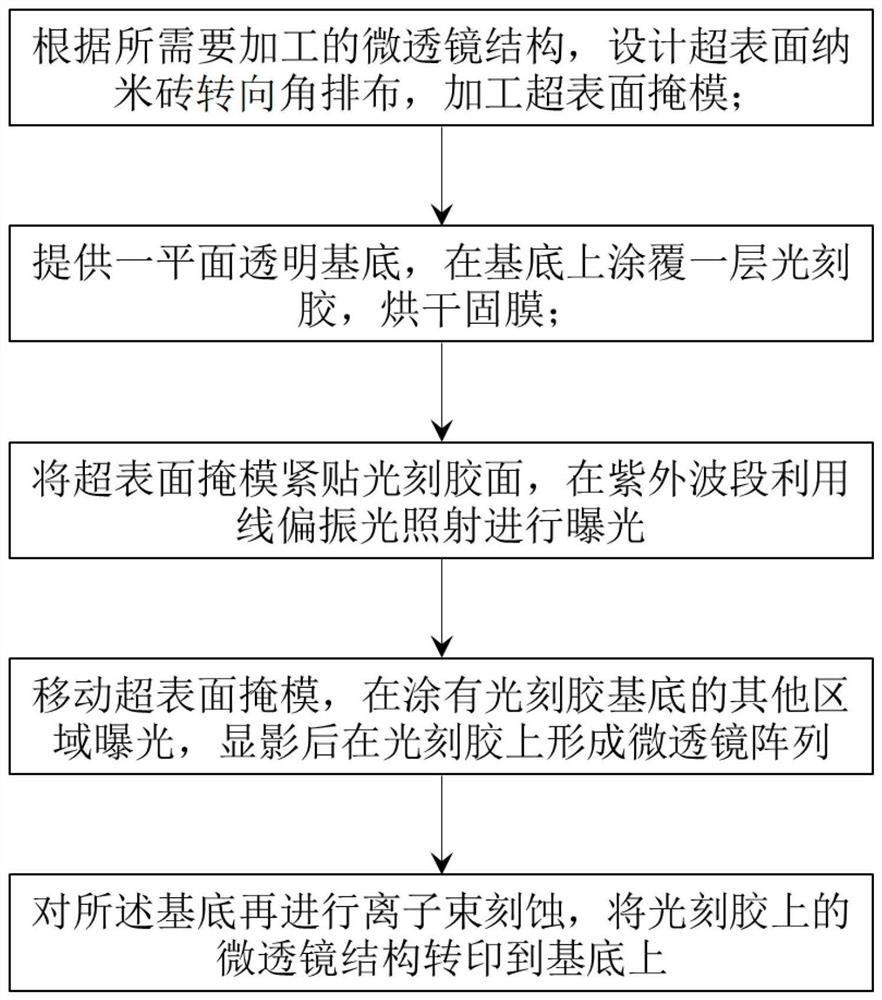
[0029] In view of the problems of limited grayscale, high production cost, and limited grayscale control level in the production of microlens arrays by the grayscale mask method in the prior art, the present invention provides a method for producing a microlens array. The production process is as follows: figure 1 shown, including the following steps:

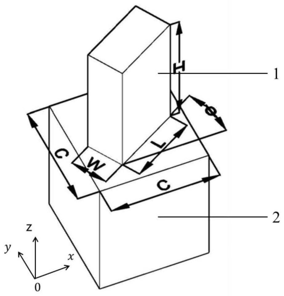
[0030] First, design and make a metasurface mask; the metasurface mask includes a nanobrick array, and the nanobrick array includes a plurality of nanobrick structural units, each nanobrick structural unit includes a working surface and nanobricks arranged on the working surface, The x-axis and y-axis are respectively set as the two sides parallel to the working surface to establish the xoy coordinate system. The...


PUM


Abstract

The invention relates to a method for manufacturing a microlens array, and the method comprises the following steps of designing and preparing a super-surface mask; providing a transparent substrate,coating a photoresist on the substrate, and drying and solidifying the film; attaching the super-surface mask to the surface of the photoresist, making the linearly polarized light in the ultravioletband incident on the super-surface mask, and performing exposure on the corresponding photoresist area under the super-surface mask; moving the super-surface mask, and performing exposure on the otherareas of the photoresist until the exposure is completed on the required areas of the photoresist; developing the substrate coated with the photoresist, and forming a microlens array structure on theexposed photoresist after development; subjecting the substrate to ion beam etching by using the microlens array structure on the photoresist as a template, and transferring the microlens array structure on the photoresist to the substrate. The method provided by the invention improves the resolution of exposure by using a super-surface instead of a traditional mask plate, can directly realize continuous and precise adjustment of exposure dose, reduces costs and improves processing accuracy.

Description

technical field [0001] The invention relates to the technical field of micro-nano optics and micro-lens array preparation, in particular to a method of using a metasurface mask instead of a traditional reticle to form a required relief profile on the surface of a photoresist by one photolithography to form a micro-lens array method. Background technique [0002] At present, miniaturization and intelligence have become a major trend in the development of modern instruments and equipment, and traditional optical components have been unable to keep up with the development requirements due to size and volume limitations. As one of the most important basic elements in the optical system, the size of the lens has an important impact on the volume of the entire optical system. Microlens arrays not only have the basic functions of traditional lenses such as focusing and imaging, but also have been widely used in the fields of optical information processing, optical computing, optic...

Claims


Application Information

Patent Timeline
Patent Type & Authority Patents(China)
IPC IPC(8): G02B3/00G03F7/00
CPCG02B3/0012G03F7/00
Inventor 郑国兴梁聪玲李子乐付娆邓联贵李仲阳
Owner WUHAN UNIV
Why Eureka
Try Eureka