Edge coupling photoelectric device packaging structure and preparation method thereof

A technology for packaging structure and optoelectronic devices, which is applied to optical components, coupling of optical waveguides, light guides, etc., can solve the problems of unsuitability for mass production of optoelectronic devices, high input cost, low efficiency, etc., and achieves easy assembly process and mass production, Small assembly error and the effect of reducing transmission loss

Pending Publication Date: 2020-01-10
NAT CENT FOR ADVANCED PACKAGING
View PDF6 Cites 8 Cited by
  • Summary
  • Abstract
  • Description
  • Claims
  • Application Information

AI Technical Summary

Problems solved by technology

[0005] Therefore, the technical problem to be solved by the present invention is to overcome the defects of high equipment investment cost, low efficiency, low yield, and unsuitability for mass production of optoelectronic devices in the active coupling alignment method in the prior art, thereby providing an edge Coupled optoelectronic device packaging structure and preparation method thereof

Method used


Image

  • Edge coupling photoelectric device packaging structure and preparation method thereof
  • Edge coupling photoelectric device packaging structure and preparation method thereof
  • Edge coupling photoelectric device packaging structure and preparation method thereof

Examples


Embodiment 1

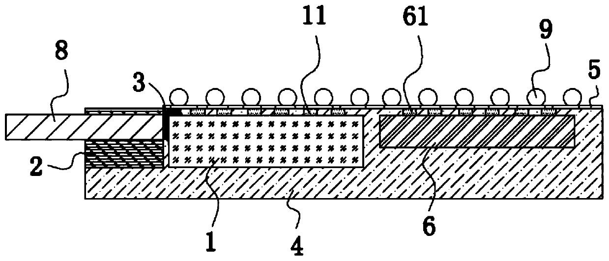
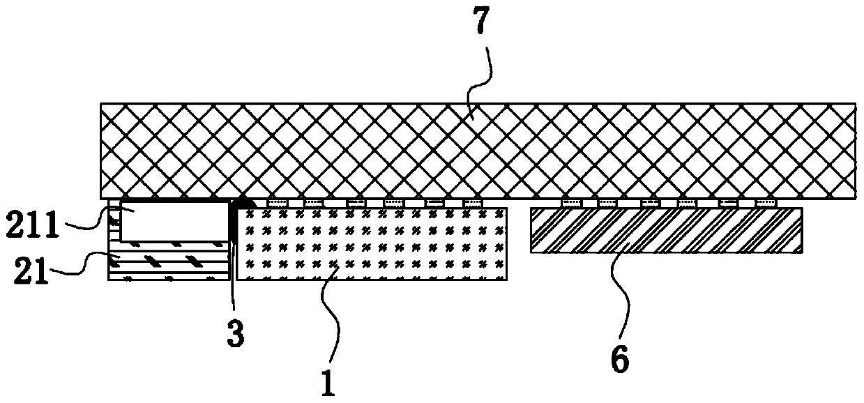
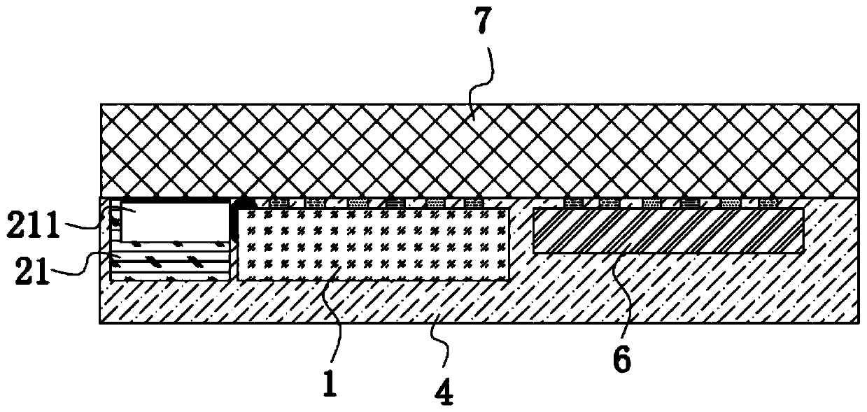
[0044] like figure 1 As shown, this embodiment relates to a packaging structure of an edge-coupled optoelectronic device, including an optical chip 1 , an optical coupling structure block 2 , a transparent resin protection structure block 3 and a packaging layer 4 .

[0045] The optical chip 1, the optical coupling structural block 2 and the transparent resin protective structural block 3 are plastic-sealed together by the encapsulation layer 4, the optical chip 1, the optical coupling structural block 2 and the transparent resin protective structural block 3 are located in the encapsulation layer 4, and the optical coupling structural block 2 is used to fix the optical fiber 8 so that the optical fiber 8 is coupled with the optical chip 1, the transparent resin protective structure block 3 is arranged between the optical chip 1 and the optical coupling structural block 2, and the transparent resin protective structural block 3 is used to protect the coupling of the optical chi...


PUM


Abstract

The invention belongs to the field of photoelectric devices and relates to an edge coupling photoelectric device packaging structure. The edge coupling photoelectric device packaging structure comprises an optical chip, an optical coupling structure block and a transparent resin protection structure block; the edge coupling structure is arranged on the optical chip; the optical coupling structureblock abuts against the side coupling structure; a through hole used for fixing an optical fiber is formed in the optical coupling structure block; the transparent resin protection structure block isarranged between the optical chip and the optical coupling structure block and is used for covering the coupling surface of the optical chip so as to ensure normal light transmission; and the opticalchip, the coupling structure block and the transparent protection resin are all located in a packaging layer. In the use process of the edge coupling photoelectric device packaging structure, it justneeds to directly insert the optical fiber into the through hole so as to be fixed, so that high-precision alignment between the optical fiber and the optical chip can be achieved. The edge couplingphotoelectric device packaging structure has the advantages of passive alignment, simple structure, high precision and easiness in assembling process and mass production.

Description

technical field [0001] The invention relates to the field of optoelectronic devices, in particular to an edge-coupled optoelectronic device packaging structure and a preparation method thereof. Background technique [0002] With the rapid development of various mobile consumer electronic products, mobile consumer electronic products have higher and higher requirements on the quality of network communication speed and delay, and optical communication technology satisfies the corresponding requirements well. Among them, in the silicon In the photosynthetic photoelectric integrated system, in order to meet the requirements of long-distance, high-bandwidth, and high-quality signal transmission, single-mode laser transmission technology is usually required. [0003] Single-mode laser transmission technology has the advantages of long-distance, high-bandwidth, and high-quality signal transmission, but the mode spot of single-mode laser is small, and its radius is only within 10 μm...

Claims


Application Information

Patent Timeline
Patent Type & Authority Applications(China)
IPC IPC(8): G02B6/42
CPCG02B6/4284
Inventor 孙瑜刘丰满曹立强
Owner NAT CENT FOR ADVANCED PACKAGING
Why Eureka
Try Eureka