Fine-pitch BGA novel packaging structure and filter capacitor design method

A technology of filter capacitors and packaging structures, applied in circuits, electrical components, electrical solid devices, etc., to achieve the effect of improving integrity and reducing impedance characteristics

Inactive Publication Date: 2020-01-10
JIANGNAN INST OF COMPUTING TECH
View PDF4 Cites 0 Cited by
  • Summary
  • Abstract
  • Description
  • Claims
  • Application Information

AI Technical Summary

Problems solved by technology

However, with the improvement of packaging integration, the packaging filter capacitor design method introduced in the above literature is aimed at the BGA package with a pin pitch of 1.0mm. Once it is used for a smaller package pin pitch, such as a If the distance is reduced to 0.8mm, the above method cannot be applied

Method used


Image

  • Fine-pitch BGA novel packaging structure and filter capacitor design method
  • Fine-pitch BGA novel packaging structure and filter capacitor design method
  • Fine-pitch BGA novel packaging structure and filter capacitor design method

Examples


Embodiment Construction

[0029] The technical solution of the present invention will be further described and illustrated through specific embodiments below, so that the technical solution will be clearer and clearer. Those skilled in the art can easily understand other advantages and effects of the present invention from the contents disclosed in this specification. The present invention can also be implemented or applied through other different specific implementation modes, and various modifications or changes can be made to the details in this specification based on different viewpoints and applications without departing from the spirit of the present invention.

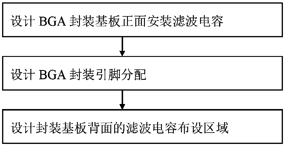
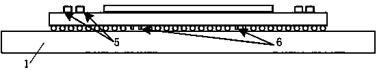
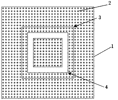
[0030] This embodiment relates to a novel packaging structure and filter capacitor design method of fine-pitch BGA, such as figure 1 As shown, the method includes the following steps:

[0031] (1) Design and install filter capacitors on the front of the BGA package substrate;

[0032] (2), design BGA package pin assignment;

[0033] (...


PUM


Abstract

The invention discloses a fine-pitch BGA novel packaging structure and filter capacitor design method. The method is characterized by comprising the following steps of: (1) designing a filter capacitor installed on the front surface of a BGA packaging substrate, (2) designing BGA packaging pin distribution, and (3) designing a filter capacitor layout area on the back surface of the packaging substrate. By adopting the novel BGA packaging structure and filter capacitor design method, the problem of packaging capacitor layout caused by height limitation of fine-pitch BGA packaging solder balls is solved, packaging back capacitance is increased for fine-pitch BGA packaging, the power supply impedance characteristic of a packaging power supply distribution system is effectively reduced, and the purpose of improving the integrity of a packaging power supply is achieved.

Description

technical field [0001] The invention belongs to the technical field of integrated circuit chip packaging, and in particular relates to a novel packaging structure of a fine-pitch BGA and a design method for a filter capacitor. Background technique [0002] VLSI (Very Large Scale Integration Circuit, VLSI) is an integrated circuit that combines a large number of transistors into a single chip, and its integration is greater than that of large scale integrated circuits. With the continuous improvement of integration, operating frequency, and computing performance of VLSI chips, the power consumption required for chip operation is also gradually increasing. At the same time, the operating voltage of the chip continues to decrease with the progress of the process, resulting in a decrease in the tolerance of the operating voltage of the chip. In order to ensure the stable and reliable operation of the chip, the power distribution system is facing severe challenges. [0003] Chip...

Claims


Application Information

Patent Timeline
Patent Type & Authority Applications(China)
IPC IPC(8): H01L21/60H01L23/64
CPCH01L23/642H01L24/14H01L2224/14131H01L2224/16225H01L2924/15311H01L2924/19105
Inventor 胡晋金利峰郑浩王彦辉李川张弓
Owner JIANGNAN INST OF COMPUTING TECH
Why Eureka
Try Eureka