Semiconductor laser spectrum beam combining device and method based on collimation-deflection element

A deflection element and spectral beam combining technology, which is applied in the direction of semiconductor laser devices, semiconductor lasers, laser devices, etc., can solve the problems of low beam combining efficiency and achieve the effects of improving efficiency, increasing output power and brightness, and stabilizing light field modes

Active Publication Date: 2020-01-10
HUAZHONG UNIV OF SCI & TECH
View PDF4 Cites 5 Cited by
  • Summary
  • Abstract
  • Description
  • Claims
  • Application Information

AI Technical Summary

Problems solved by technology

[0006] For the above defects or improvement needs of the prior art, the object of the present invention is to provide a semiconductor laser spectral beam combining device and method based on collimation-deflection elements, wherein through the composition of each component in the semiconductor laser spectral beam combining device and Their settings, internal structure, etc. are improved, and the overall processing process of the corresponding beam combining method is controlled. Compared with the existing technology, it can effectively solve the problems such as off-center emission in the traditional semiconductor laser array spectral beam combining method. The light beams emitted by the units are fed back and the efficiency of beam

Method used


Image

  • Semiconductor laser spectrum beam combining device and method based on collimation-deflection element
  • Semiconductor laser spectrum beam combining device and method based on collimation-deflection element
  • Semiconductor laser spectrum beam combining device and method based on collimation-deflection element

Examples


Embodiment 1

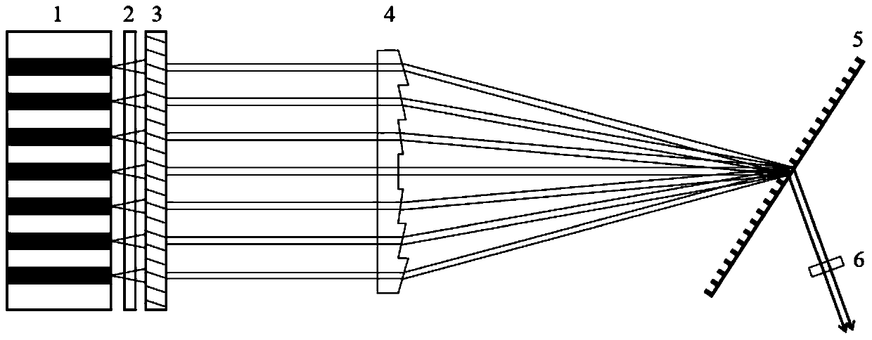
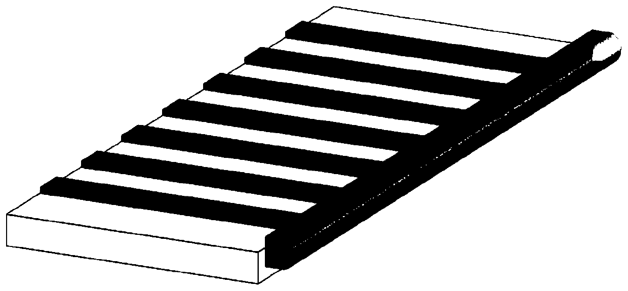
[0049] Examples of the present invention are figure 1 As shown, the device includes: a semiconductor laser array 1 , a fast-axis collimator mirror 2 , a beam rotation element 3 , a collimation-deflection element 4 , a diffraction grating 5 , and an output coupling mirror 6 .

[0050] At first the principle of the present invention is set forth:

[0051] On the whole, each light-emitting unit on the semiconductor laser array 1 can be regarded as a central light-emitting unit that translates a certain distance along the x direction. When the central light-emitting unit is translated, the light beam satisfies the grating equation mλ=d(sinα+sinβ). The diffracted beam must be perpendicular to the output coupling mirror to feed back and form a stable single longitudinal mode oscillation, that is, the diffraction angle β is a constant value during the translation process. Therefore, as α changes during translation, λ changes accordingly. If several light-emitting units are placed ...


PUM

PropertyMeasurementUnit
Number of threadsaaaaaaaaaa

Abstract

The invention belongs to the technical field of semiconductor laser, and discloses a semiconductor laser spectrum beam combining device and method based on a collimation-deflection element. The devicecomprises a semiconductor laser array (1), and a fast axis collimating mirror (2), a light beam rotating element (3), a collimation-deflection element (4), a diffraction grating (5) and an output coupling mirror (6) which are sequentially arranged along a light path, wherein the collimation-deflection element (4) is used for refracting light beams emitted by different emission units and enablingthe light beams to enter the same area of the diffraction grating (5), and the diffraction grating (5) is used for diffracting a plurality of light beams overlapped in the same area at the same diffraction angle, so that the light beams become the same light beam and are outputted. Thus, by improving the composition of each component in the beam combining device, the arrangement mode and the internal structure of each component and the like, the problems of feedback of light beams emitted by an off-center emission unit, low beam combining efficiency and the like in the traditional semiconductor laser array spectrum beam combining mode can be effectively solved.

Description

technical field [0001] The invention belongs to the technical field of semiconductor lasers, and more specifically relates to a semiconductor laser spectral beam combining device and method based on a collimation-deflection element, and is a novel semiconductor laser array spectral beam combining system and beam combining method. Background technique [0002] With the rapid development of the field of laser science, one of the important issues is to achieve high-power, high-brightness laser output. [0003] Semiconductor lasers are widely used in communication, biology, medical treatment and material processing due to their advantages such as wide range of wavelength selection, small size, high electro-optic energy conversion rate and long working life. But its shortcomings are also obvious: low power of a single light-emitting unit, poor beam quality in the slow axis direction leads to low beam energy density, etc. These shortcomings hinder the direct use of semiconductor l...

Claims


Application Information

Patent Timeline
IPC IPC(8): H01S5/40
CPCH01S5/4012H01S5/4025
Inventor 唐霞辉马豪杰陈子康张旭辉罗惜照肖瑜秦应雄万辰皓
Owner HUAZHONG UNIV OF SCI & TECH
Why Eureka
Try Eureka