Semiconductor device and forming method thereof

A semiconductor and device technology, applied in the field of semiconductor structure and its formation, can solve the problems of the performance of semiconductor devices need to be improved, the reliability of the device is reduced, the thermal breakdown of the gate dielectric layer, etc., to achieve improved breakdown resistance, improved reliability, and improved The effect of the interface layer

Active Publication Date: 2020-01-14
SEMICON MFG INT (SHANGHAI) CORP +1
View PDF7 Cites 0 Cited by
  • Summary
  • Abstract
  • Description
  • Claims
  • Application Information

AI Technical Summary

Problems solved by technology

[0003] With the continuous development of integrated circuit technology, the size of MOS devices shrinks accordingly, and the lateral electric field in the channel increases, causing a large number of hot carriers to increase, resulting in an increase in the possibility of hot carriers entering the gate dielectric layer, and the gate dielectric layer is easy to Thermal runaway occurs, reducing the reliability of the device
[0004] The performance of semiconductor devices composed of field effect transistors in the prior art needs to be improved

Method used


Image

  • Semiconductor device and forming method thereof
  • Semiconductor device and forming method thereof
  • Semiconductor device and forming method thereof

Examples


Embodiment Construction

[0030] As mentioned in the background, the performance of semiconductor devices formed in the prior art needs to be improved.

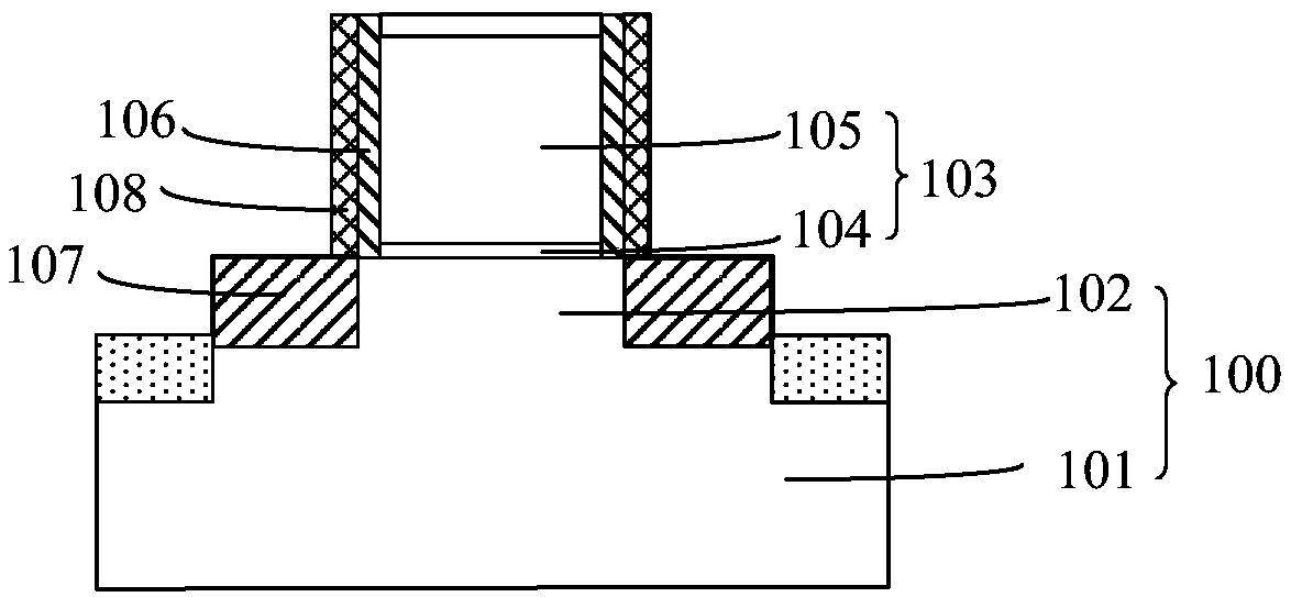
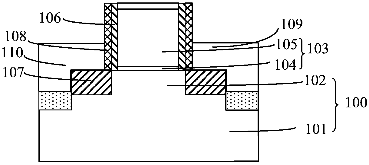
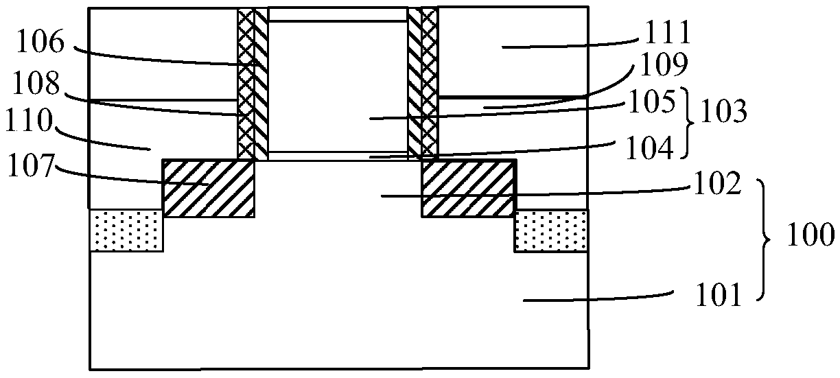
[0031] A method for forming a semiconductor device, comprising: providing a semiconductor substrate with a dummy gate structure on the semiconductor substrate, the dummy gate structure including a dummy gate dielectric layer and a dummy gate electrode layer positioned on the dummy gate dielectric layer , there are source and drain doped regions on the substrate on both sides of the dummy gate structure, and there is an interlayer dielectric layer on the source and drain doped regions and the dummy gate structure; the dummy gate electrode layer is removed until exposed On the top surface of the dummy gate dielectric layer, an opening is formed in the interlayer dielectric layer; a gate dielectric layer is formed on the sidewall of the opening and the surface of the dummy gate dielectric layer; after the gate dielectric layer is formed, the opening is I...


PUM

PropertyMeasurementUnit
thicknessaaaaaaaaaa
thicknessaaaaaaaaaa

Abstract

The invention provides a method for forming a semiconductor device. The method comprises the steps that a semiconductor substrate with a dummy gate structure thereon is provided, wherein the dummy gate structure comprises a dummy gate dielectric layer and a dummy gate electrode layer on the dummy gate dielectric layer, and a source region and a drain region are in the substrate on both sides of the dummy gate structure; an interlayer dielectric layer is formed on the semiconductor substrate, the source region and the drain region, and the interlayer dielectric layer covers the sidewall of thedummy gate structure; the dummy gate electrode layer is removed until the top surface of the dummy gate dielectric layer is exposed; an opening is formed in the interlayer dielectric layer, wherein the opening comprises a first region adjacent to the drain region; a gate dielectric layer is formed on the sidewall of the opening and the surface of the dummy gate dielectric layer; after the gate dielectric layer is formed, first ion implantation is carried out on the gate dielectric layer of the first region; and improving ions are used for filling defects and atomic gaps of the gate dielectriclayer. The reliability of the semiconductor device formed by the method is better.

Description

technical field [0001] The invention relates to the field of semiconductor manufacturing, in particular to a semiconductor structure and a forming method thereof. Background technique [0002] MOS (Metal-Oxide-Semiconductor) transistor is one of the most important elements in modern integrated circuits. The basic structure of MOS transistors includes: a semiconductor substrate; a gate structure located on the surface of the semiconductor substrate, and the gate structure includes : a gate dielectric layer on the surface of the semiconductor substrate and a gate electrode layer on the surface of the gate dielectric layer; source and drain doped regions in the semiconductor substrate on both sides of the gate structure. [0003] With the continuous development of integrated circuit technology, the size of MOS devices shrinks accordingly, and the lateral electric field in the channel increases, causing a large number of hot carriers to increase, resulting in an increase in the ...

Claims


Application Information

Patent Timeline
Patent Type & Authority Applications(China)
IPC IPC(8): H01L21/265H01L21/28H01L29/78H01L21/336
CPCH01L21/265H01L21/28008H01L29/66477H01L29/78
Inventor 赵猛
Owner SEMICON MFG INT (SHANGHAI) CORP
Why Eureka
Try Eureka