Check patentability & draft patents in minutes with Patsnap Eureka AI!

Gate voltage bootstrap switching circuit adopting CMOS transmission gate

A gate voltage bootstrap and switching circuit technology, applied in the field of microelectronics, can solve problems such as the inability to maintain gate-source voltage stability

Active Publication Date: 2020-01-14
CHONGQING UNIV OF POSTS & TELECOMM
View PDF3 Cites 4 Cited by
  • Summary
  • Abstract
  • Description
  • Claims
  • Application Information

AI Technical Summary

Problems solved by technology

A gate-voltage bootstrap switch circuit using CMOS transmission gate is proposed to solve the problem that the traditional circuit cannot maintain the stability of the gate-source voltage when the input signal is low, thereby improving the linearity and dynamic characteristics of the gate-voltage bootstrap switch

Method used


Image

  • Gate voltage bootstrap switching circuit adopting CMOS transmission gate
  • Gate voltage bootstrap switching circuit adopting CMOS transmission gate

Examples


Embodiment Construction

[0013] The technical solutions in the embodiments of the present invention will be described clearly and in detail below with reference to the drawings in the embodiments of the present invention. The described embodiments are only some of the embodiments of the invention.

[0014] The technical scheme that the present invention solves the problems of the technologies described above is:

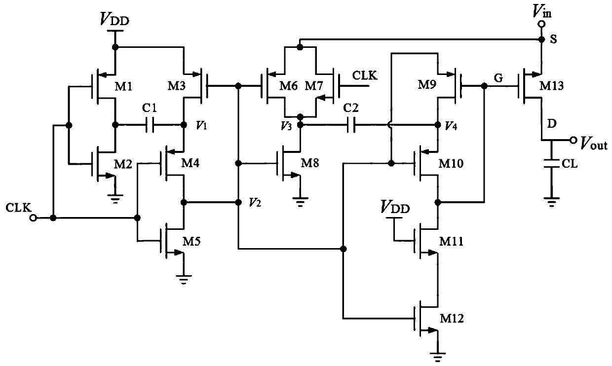
[0015] In the embodiment of the present application, the input voltage is fed back to the gate of the switching transistor (NMOS transistor M13 ) through the CMOS transmission gate (PMOS transistor M6 and NMOS transistor M7 ), the bootstrap capacitor C2 and the PMOS transistor M10 . Thereby realizing the high linearity of the gate voltage bootstrap switch in the whole input range. CMOS transmission gate (Transmission Gate) is a controllable switch circuit that can transmit both digital signals and analog signals. The CMOS transmission gate is composed of a PMOS and an NMOS transistor conne...


PUM


Abstract

The invention discloses a gate voltage bootstrap switching circuit adopting a CMOS transmission gate. The gate voltage bootstrap switching circuit comprises a switching tube, a control logic circuit,a bootstrap capacitor and a load capacitor. The control logic circuit comprises an NMOS tube M1, a PMOS tube M2, a PMOS tube M3, a PMOS tube M4, an NMOS tube M5, a PMOS tube M6, an NMOS tube M7, an NMOS tube M8, a PMOS tube M9, a PMOS tube M10, an NMOS tube M11 and an NMOS tube M12. The bootstrap capacitor comprises a capacitor C1 and a capacitor C2. The objective of the invention is to improve the linearity and the signal-to-noise ratio of the switching circuit. The innovation lies in that CMOS transmission gates (M6 and M7) are used for feeding back input voltage to the grid electrode of theswitching tube, so that the grid source voltage of the switching tube is kept constant, the NMOS switching tube becomes a constant-value resistor in the sampling stage, and therefore the high-performance grid voltage bootstrap switching circuit is achieved.

Description

technical field [0001] The invention belongs to the technical field of microelectronics, and in particular relates to a high-performance grid voltage bootstrap switch circuit. Background technique [0002] The switch circuit is an important module in the integrated circuit system. The main function of the switch circuit is to follow the external signal conversion in the follow-up phase and keep the signal unchanged in the hold phase. It is widely used in circuits related to signal acquisition, including ADC In the circuit, a follow-and-hold circuit and a sample-and-hold circuit can be implemented. [0003] The basic idea of ​​the traditional gate voltage bootstrap switch structure is to charge the capacitor C1 during the sampling phase, and the voltage of V1 rises to V DD , continue to charge the capacitor C1 during the hold phase, and the voltage of V1 rises to 2V DD , and feed back through the NMOS tube, so that the switch tube is in the following phase, and the gate-sou...

Claims


Application Information

Patent Timeline
Patent Type & Authority Applications(China)
IPC IPC(8): H03K17/687H03M1/12
CPCH03K17/687H03M1/1245
Inventor 袁军唐晓斌周怡王巍赵汝法
Owner CHONGQING UNIV OF POSTS & TELECOMM
Features
  • R&D
  • Intellectual Property
  • Life Sciences
  • Materials
  • Tech Scout
  • Unparalleled Data Quality
  • Higher Quality Content
  • 60% Fewer Hallucinations
Learn More