Method for manufacturing semiconductor element
A semiconductor and component technology, applied in the field of making dynamic random access memory components
- Summary
- Abstract
- Description
- Claims
- Application Information
AI Technical Summary
Problems solved by technology
Method used
Image

Examples
Embodiment Construction
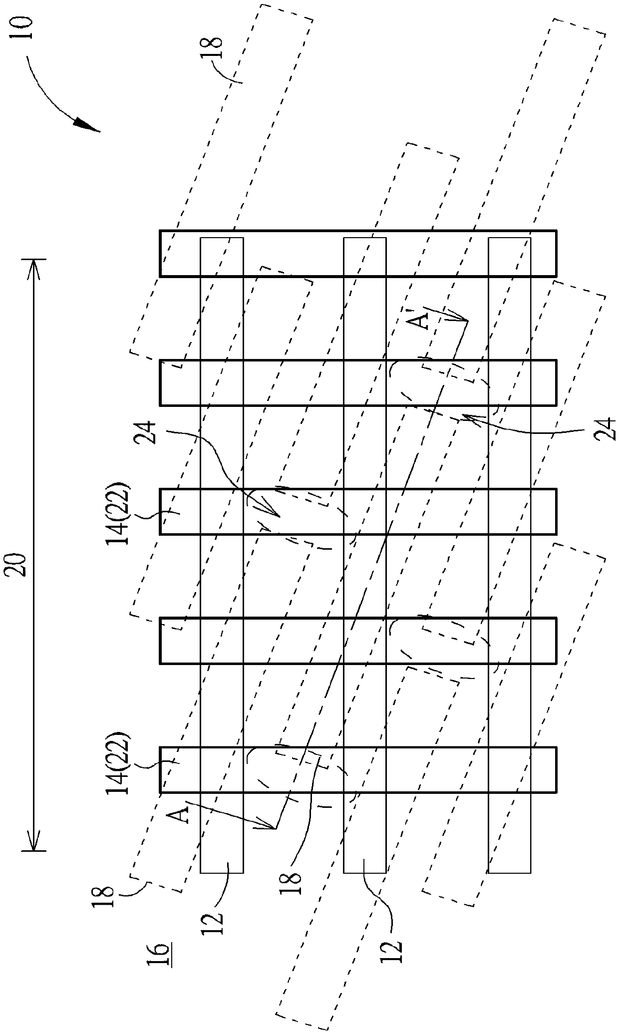
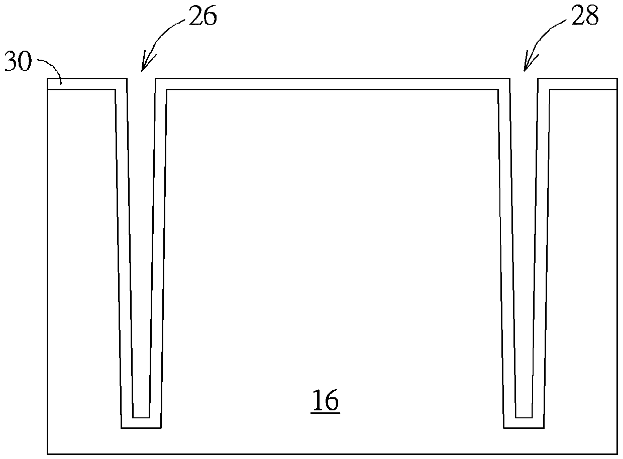
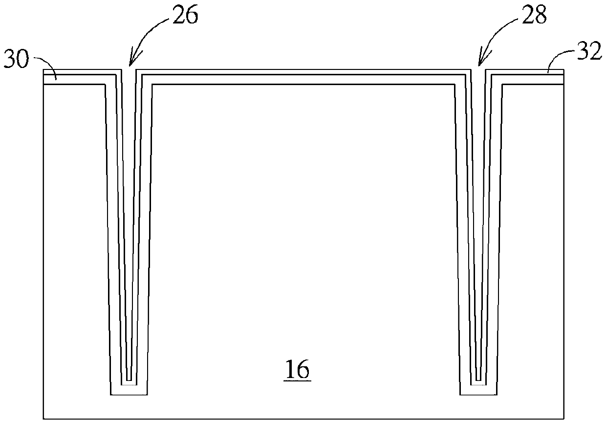
[0027] Please refer to Figure 1 to Figure 5 , Figure 1 to Figure 5 A schematic diagram of a method for making a dynamic random access memory element in a preferred embodiment of the present invention, wherein figure 1 for top view, Figure 2 to Figure 5 show figure 1 A schematic diagram of a method for fabricating shallow trench isolation of dynamic random access memory elements along the tangent line AA' in the figure. This embodiment provides a memory element, such as a DRAM element 10 with a recessed gate, which includes at least one transistor element (not shown) and at least one capacitor structure (not shown), so as to As the minimum constituent unit in the DRAM array, it receives voltage signals from the bit line 12 and the word line 14 .
[0028] Such as figure 1 As shown, the DRAM device 10 includes a substrate 16, such as a semiconductor substrate made of silicon, and then at least one shallow trench isolation 24 is formed in the substrate 16 to define a plura...
PUM
| Property | Measurement | Unit |
|---|---|---|
| electron work function | aaaaa | aaaaa |
Abstract
Description
Claims
Application Information
 - R&D
- Intellectual Property
- Life Sciences
- Materials
- Tech Scout
- Unparalleled Data Quality
- Higher Quality Content
- 60% Fewer Hallucinations
Browse by: Latest US Patents, China's latest patents, Technical Efficacy Thesaurus, Application Domain, Technology Topic, Popular Technical Reports.
© 2025 PatSnap. All rights reserved.Legal|Privacy policy|Modern Slavery Act Transparency Statement|Sitemap|About US| Contact US: help@patsnap.com