Intelligent factory for semiconductor packaging test

A technology for packaging and testing semiconductors, which is applied in semiconductor/solid-state device testing/measurement, semiconductor/solid-state device manufacturing, electrical components, etc., and can solve the problem of compound robot semiconductor material boxes and intelligent fixed material racks that do not have open access to semiconductor materials and other issues, to achieve the effect of material transmission routing and solve the effects of diversity and complexity

Active Publication Date: 2020-01-24
SHENZHEN STS MICROELECTRONICS
View PDF18 Cites 2 Cited by
  • Summary
  • Abstract
  • Description
  • Claims
  • Application Information

AI Technical Summary

Problems solved by technology

[0005] These smart factories or workshops in the prior art are not directly used in the field of semiconductor chip packaging and testing, and there are no composite robots that openly access semiconductor materials, material boxes for semiconductors, intelligent fixed material racks, etc.

Method used


Image

  • Intelligent factory for semiconductor packaging test
  • Intelligent factory for semiconductor packaging test
  • Intelligent factory for semiconductor packaging test

Examples


no. 1 approach

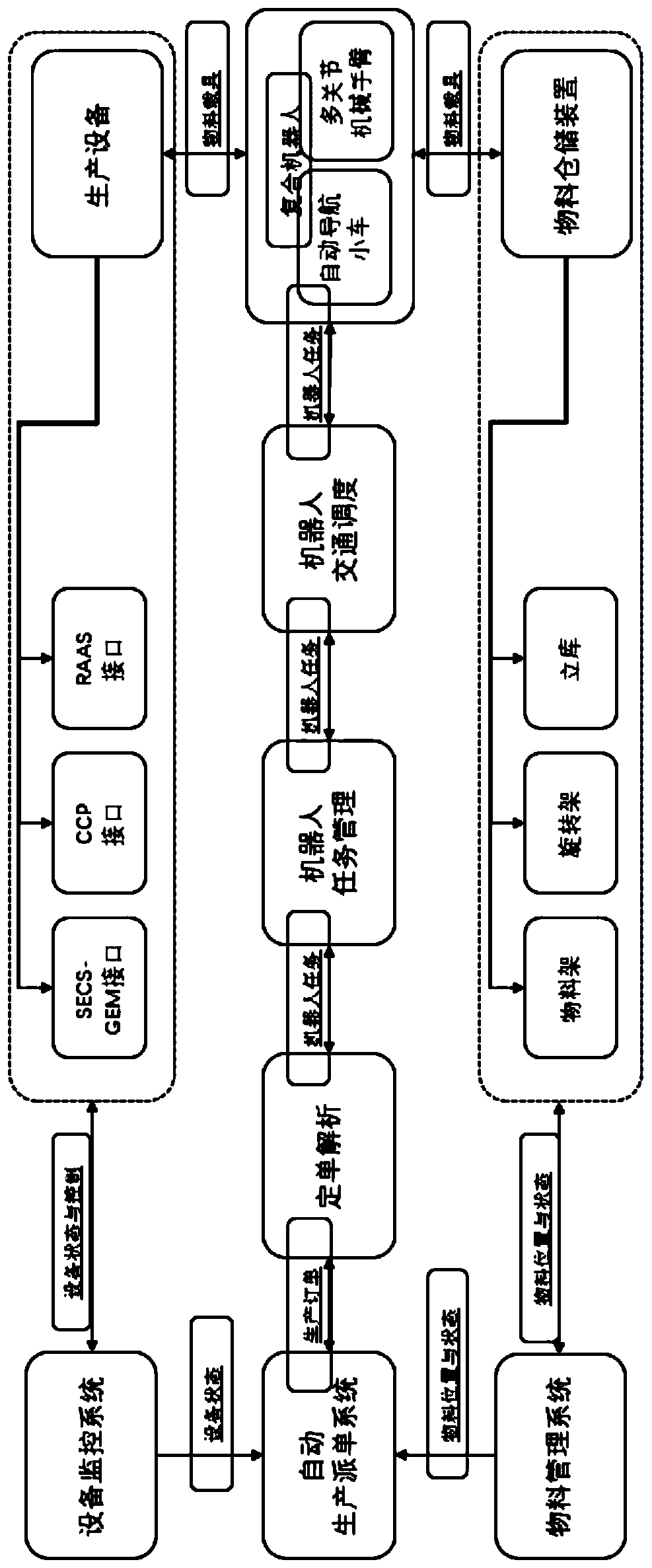
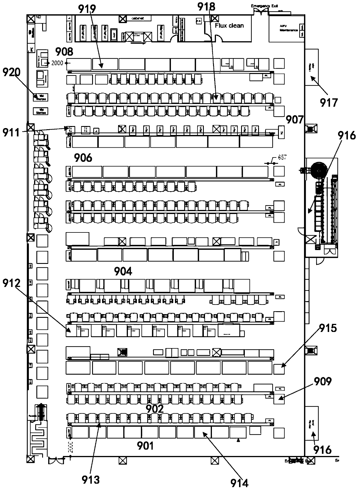
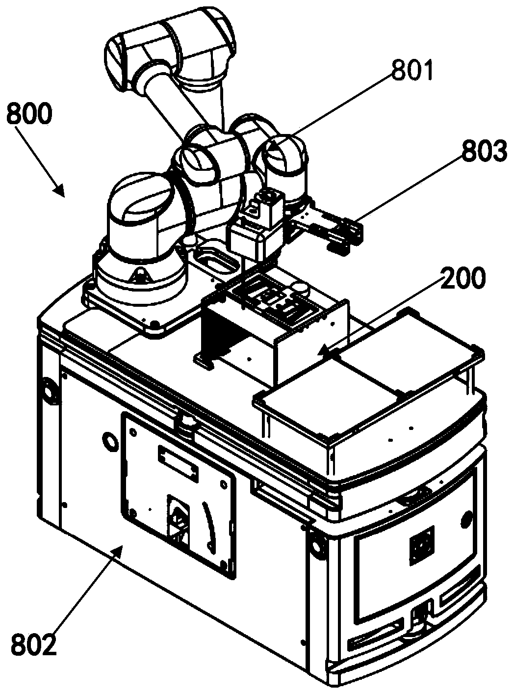
[0062] Based on the above-mentioned inventive concept, with reference to Figures 1 to 12 , according to the first embodiment of the semiconductor packaging and testing smart factory of the present invention, the semiconductor packaging and testing smart factory can automatically transfer materials between production stations in different process steps. refer to figure 2 , each row of the factory workshop includes multiple workstations of the same type. But different rows can correspond to different types of workstations. That is to say, before the present invention, the material handling between different rows needs to be carried out manually. After the implementation of the present invention, the material handling between different rows is realized by a composite robot, so as to achieve the purpose of improving the degree of automation. refer to figure 1 , the semiconductor packaging and testing intelligent factory includes a composite robot, production equipment, materi...

no. 2 approach

[0176] As one of the key points of the invention of this patent application, the facility layout of the semiconductor packaging and testing smart factory can be arranged in various ways, refer to Figures 1 to 12 , according to the second embodiment of the semiconductor packaging and testing smart factory of the present invention, the semiconductor packaging and testing smart factory includes a material carrier, a composite robot, production equipment, and a material storage device;

[0177] The composite robot can take out materials from the material storage device, and transport the materials to the production equipment by means of the material carrier, or, the composite robot can extract materials from the production equipment in the first process step taking out the material, and transporting the material to the production equipment of the second process step by means of the material carrier;

[0178] The material storage device includes a fixed material rack, a rotating m...


PUM


Abstract

The invention discloses an intelligent factory for semiconductor packaging test. With the intelligent factory adopted, materials can be automatically conveyed between the production stations of different process steps. The intelligent factory comprises a composite robot, production equipment, a material storage device, an equipment monitoring system, an automatic production order dispatching system and a material management system; the equipment monitoring system can monitor the equipment state and event information of the production equipment through an equipment communication interface and transmit a control instruction; the material management system can communicate with the material storage device to obtain material position and state information; the automatic production order dispatching system can generate a production order and a robot task according to the equipment state and event information and the material position and state information; and the composite robot can take out materials from the material storage device according to the robot task. Unmanned full-automatic chip packaging and testing are basically realized in the intelligent factory.

Description

technical field [0001] The present invention relates to the technical field of program control systems for comprehensive factories (G05B 19 / 418), and in particular, the present invention relates to semiconductor packaging and testing smart factories. Background technique [0002] In the semiconductor packaging and testing production process, due to the variety of product types, complex processes and a large amount of information and data, a large number of production personnel in different positions are required to operate production equipment and transport materials according to the production process. Therefore, in semiconductor packaging and testing manufacturing, although the process production uses advanced automated process equipment, due to the particularity of the process, it is impossible to carry out assembly line operations between processes, and the traditional semiconductor packaging and testing factory has not reached a real intelligent unmanned factory. [000...

Claims


Application Information

Patent Timeline
Patent Type & Authority Applications(China)
IPC IPC(8): H01L21/66H01L21/673H01L21/68
CPCH01L21/673H01L21/68H01L22/12
Inventor 罗家绍张震虞涛余波吴迪喻宁梁承财汪世军高伟淦
Owner SHENZHEN STS MICROELECTRONICS
Why Eureka
Try Eureka