High-quality seed crystal wafer cultivation method for artificial quartz crystal

A quartz crystal and seed crystal technology is applied in the field of frame-shaped +X-direction crystal growth of artificial quartz crystals and the manufacture of seed wafers.

Active Publication Date: 2020-02-04
山东博达光电有限公司
View PDF5 Cites 0 Cited by
  • Summary
  • Abstract
  • Description
  • Claims
  • Application Information

AI Technical Summary

Problems solved by technology

[0005] In the document "NEW TECHNIQUE TO DECREASE DISLOCATION IN SYNTHETIC QUARTZ CRYSTAL", the technical principle of the frame seed crystal method is explained and affirmed, but the document does not have a specific description of the processing of the frame seed wafer; therefore, how to operate in order to realize the cultivation of artificial quartz High-quality seeds of crystals, currently unknown

Method used


Image

  • High-quality seed crystal wafer cultivation method for artificial quartz crystal
  • High-quality seed crystal wafer cultivation method for artificial quartz crystal
  • High-quality seed crystal wafer cultivation method for artificial quartz crystal

Examples


Embodiment 1

[0057] Step 1. The artificial quartz crystal is first cut into a frame-shaped crystal that only retains part of the positive and negative axis areas (cutting the frame crystal):

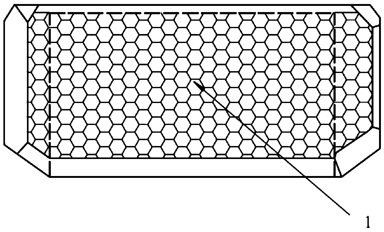
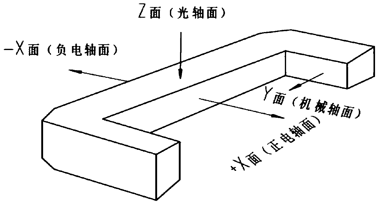
[0058] Artificial quartz crystals to be cut (such as figure 1 ), the crystal length (Y) is about 230mm; the crystal thickness (Z) is about 75mm; the crystal width (X) is about 100mm.

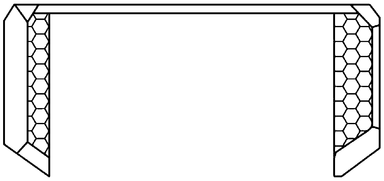
[0059] Artificial quartz crystals to be cut (such as figure 1 One Z surface (optical axis surface) and +X surface (positive electric axis surface) are ground, and the orientation accuracy of the ground two planes is guaranteed to be within ±10'; on the other unground Z surface (optical axis surface) ) to draw the part that needs to be cut off --- cut off part 1, that is, according to the common sense of this industry, draw according to the different growth mounds and regional boundaries of the Z zone and the X zone on the unground Z surface (optical axis surface) The width of the X region to be reserved is enough; th...


PUM

PropertyMeasurementUnit
lengthaaaaaaaaaa
thicknessaaaaaaaaaa

Abstract

The invention discloses a high-quality seed crystal wafer cultivation method for an artificial quartz crystal. The method comprises the following steps: 1, cutting the artificial quartz crystal to becut to form a frame crystal only reserving a part of positive and negative electric axis areas; 2, cutting the frame crystal to form frame seed crystal wafers; 3, putting the frame seed crystal wafersinto a high-pressure kettle, and growing the crystal; and 4, cutting the grown part of the frame crystal to obtain the high-quality seed crystal wafer. The characteristic that the crystal grown in the +X direction (positive electric axis direction) of the quartz crystal does not inherit the defects of the seed crystal wafer is utilized to cultivate the high-quality seed crystal wafer is cultivated, and the seed crystal wafer cutting is carried out on the grown part of the crystal, so that the high-quality seed crystal wafer with a low corrosion tunnel density is obtained.

Description

technical field [0001] The invention relates to a high-quality seed wafer cultivation process of an artificial quartz crystal, in particular to a frame-shaped +X direction (positive electric axis direction) crystal growth of an artificial quartz crystal and a seed wafer manufacturing technology. Background technique [0002] Artificial quartz crystal has good piezoelectric and optical properties, and is an important crystal material in the fields of electronics and optics. [0003] Artificial quartz crystals are grown on seed wafers by hydrothermal temperature difference method. The earliest seed wafers were cut from natural quartz crystals. Difficult, the current seed wafer is cut from the artificial quartz crystal; however, due to the crystalline characteristics of the artificial quartz crystal, the defects on the seed wafer will be inherited to the grown crystal. Cutting the seed wafer in the quartz crystal causes more and more lattice and corrosion tunnel defects in the...

Claims


Application Information

Patent Timeline
Patent Type & Authority Applications(China)
IPC IPC(8): C30B7/10C30B29/18B28D5/04
CPCB28D5/04B28D5/042C30B7/10C30B29/18
Inventor 刘盛浦易际让王晓刚
Owner 山东博达光电有限公司
Why Eureka
Try Eureka