Isolating film, top-emitting photoelectric device and manufacturing method and application thereof

A technology for optoelectronic devices and manufacturing methods, applied in semiconductor/solid-state device manufacturing, electrical solid-state devices, electrical components, etc., can solve problems such as stability and lifespan to be improved, poor light extraction rate and light purity, etc., to improve light extraction efficiency. and luminous purity, good mechanical properties and chemical stability, luminous efficiency and improved light purity

Inactive Publication Date: 2020-02-04
TCL CORPORATION
View PDF6 Cites 1 Cited by
  • Summary
  • Abstract
  • Description
  • Claims
  • Application Information

AI Technical Summary

Problems solved by technology

[0005] The purpose of the present invention is to provide an isolation film, a top-emitting optoelectronic device and its preparation method, aiming to solve the problems of poor light extraction rate and light purity, stability and service life of optoelectronic devices in the thin film packaging of existing optoelectronic devices.

Method used


Image

  • Isolating film, top-emitting photoelectric device and manufacturing method and application thereof
  • Isolating film, top-emitting photoelectric device and manufacturing method and application thereof

Examples


Embodiment 1

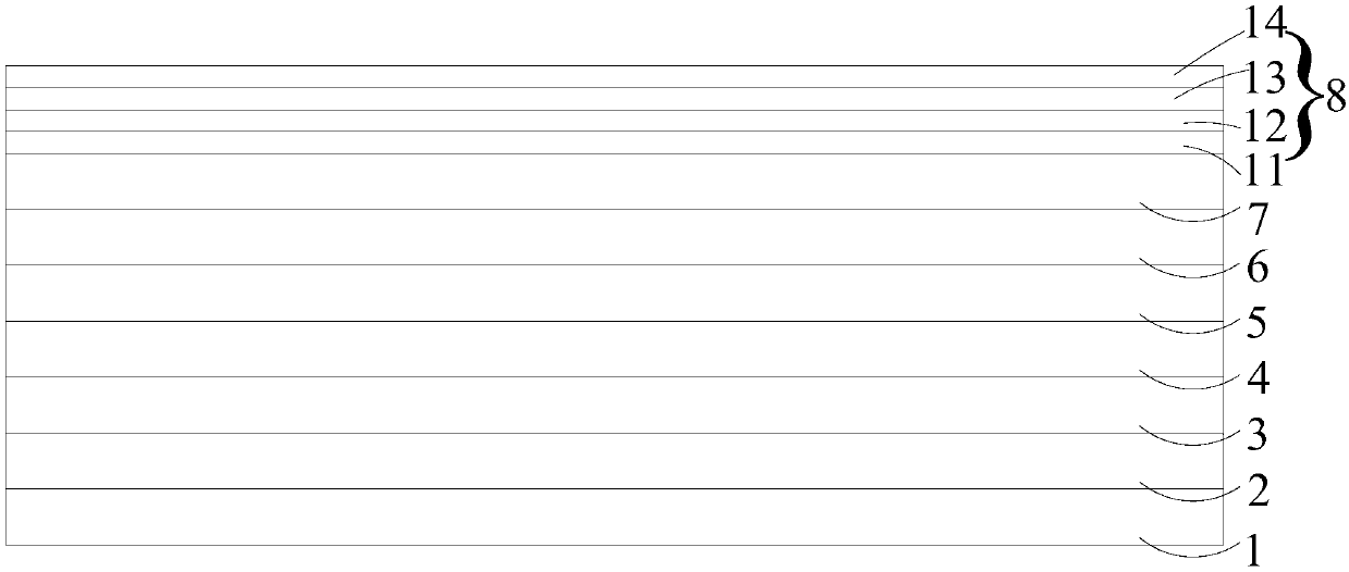
[0069] A top-emitting photoelectric device, comprising a substrate, and an Al / ITO electrode, a hole injection layer, a hole transport layer, a quantum dot light-emitting layer, an electron transport layer, a top electrode, and an encapsulation layer stacked outward from a surface of the substrate ;

[0070] Wherein, the thickness of Al / ITO electrode is 50nm;

[0071] The hole injection layer is made of PEDOT:PSS with a thickness of 50nm;

[0072] The material of the hole transport layer is poly-TPD, and its thickness is 30nm;

[0073] The material of the quantum dot light-emitting layer is CdSe / ZnS, and its thickness is 20nm;

[0074] The material of the electron transport layer is ZnO, and its thickness is 30nm;

[0075] The material of the top electrode is a magnesium-silver alloy with a thickness of 30nm;

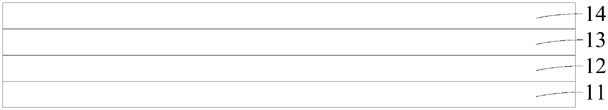
[0076] The thickness of the encapsulation layer is 125nm;

[0077]The encapsulation layer is a layer of composite film layer, and the composite film layer is sequen...

Embodiment 2

[0084] A top-emitting photoelectric device, comprising a substrate, and an Al / ITO electrode, a hole injection layer, a hole transport layer, a quantum dot light-emitting layer, an electron transport layer, a top electrode, and an encapsulation layer stacked outward from a surface of the substrate ;

[0085] Wherein, the thickness of Al / ITO electrode is 50nm;

[0086] The hole injection layer is made of PEDOT:PSS with a thickness of 50nm;

[0087] The material of the hole transport layer is poly-TPD, and its thickness is 30nm;

[0088] The material of the quantum dot light-emitting layer is CdZnS / ZnSe, and its thickness is 20nm;

[0089] The material of the electron transport layer is ZnO, and its thickness is 30nm;

[0090] The material of the top electrode is magnesium-silver alloy, and its thickness is 50nm;

[0091] The thickness of the encapsulation layer is 270nm;

[0092] The encapsulation layer is a layer of composite film layer, and the composite film layer is seq...

Embodiment 3

[0099] A top-emitting photoelectric device, comprising a substrate, and an Al / ITO electrode, a hole injection layer, a hole transport layer, a quantum dot light-emitting layer, an electron transport layer, a top electrode, and an encapsulation layer stacked outward from a surface of the substrate ;

[0100] Wherein, the thickness of Al / ITO electrode is 50nm;

[0101] The hole injection layer is made of PEDOT:PSS with a thickness of 50nm;

[0102] The material of the hole transport layer is poly-TPD, and its thickness is 30nm;

[0103] The material of the quantum dot light-emitting layer is CdS / ZnSe, and its thickness is 20nm;

[0104] The material of the electron transport layer is ZnO, and its thickness is 30nm;

[0105] The material of the top electrode is a magnesium-silver alloy with a thickness of 30nm;

[0106] The thickness of the encapsulation layer is 200nm;

[0107] The encapsulation layer is a layer of composite film layer, and the composite film layer is seque...


PUM

PropertyMeasurementUnit
thicknessaaaaaaaaaa
thicknessaaaaaaaaaa
thicknessaaaaaaaaaa

Abstract

The present invention relates to the technical field of photoelectric devices, and specifically provides an isolating film, a top-emitting photoelectric device and a manufacturing method and an application thereof. The isolating film includes a first oxide film and a metal film, a second oxide film and a third oxide film that are stacked outward from the surface of the first oxide film. The top-emitting photoelectric device includes a top electrode and a packaging layer stacked on the surface of the top electrode. The packaging layer is the isolating film. The isolating film of the invention has good mechanical properties and chemical stability, plays a good isolation effect on water vapor and oxygen and can effectively prevent penetration of water vapor and / or oxygen. When the isolating film is used as the packaging layer of the top-emitting photoelectric device, the light emission efficiency and light purity of the top-emitting photoelectric device are greatly improved, so it is conducive to improving the stability, service life and efficiency of the photoelectric device.

Description

technical field [0001] The invention belongs to the technical field of photoelectric devices, and in particular relates to an isolation film, a top-emitting photoelectric device, a manufacturing method and an application thereof. Background technique [0002] The main reason for the shortened lifetime of photovoltaic devices is the adsorption of oxygen and moisture in the air. Oxygen and / or moisture in the environment penetrate into the device, which will accelerate the aging of the device and reduce the life of the device. In order to prevent oxygen and / or moisture from entering the interior of the device, the current common method is to protect the organic film and metal electrodes through the packaging process from the influence of the outside air, and finally achieve the purpose of prolonging the life of the device. Because of this, the pros and cons of the packaging process will seriously affect the service life of optoelectronic devices. [0003] The traditional opto...

Claims


Application Information

Patent Timeline
Patent Type & Authority Applications(China)
IPC IPC(8): H01L51/52H01L51/56
CPCH10K50/844H10K71/00
Inventor 朱佩向超宇罗植天张滔李乐
Owner TCL CORPORATION
Why Eureka
Try Eureka