Optical deflection microscopic surface measuring device and method

A surface measurement and optical technology, applied in the field of measurement, can solve problems such as being susceptible to environmental interference, limited measurement range, and small measurement range, and achieve the effects of improving low spatial resolution, improving measurement accuracy, and simplifying calibration work

Active Publication Date: 2020-02-07
CHINA JILIANG UNIV
View PDF10 Cites 5 Cited by
  • Summary
  • Abstract
  • Description
  • Claims
  • Application Information

AI Technical Summary

Problems solved by technology

However, the optical interferometer measurement method has disadvantages such as small measurement dynamic range, susceptibility to environmental interference, and high detection cost.
Scanning microscopy measurement methods, such as transmission electron microscopy (STEM), have extremely high horizontal and vertical resolution, but their measurement range is small and the detection cost is high, so they are subject to many limitations in engineering surface measurement
[0003] The Chinese patent application publication number is CN107560564A, an invention patent of a free-form surface detection method and system. This patent uses a traditional optical deflection measurement device, which uses a projection screen, a component to be tested, and a CCD detector to form a reverse Hartmann optical detection. system, although the system can achieve rapid measurement of the surface of the component, but its spatial resolution is low, and it cannot achieve accurate microscopic measurement
A device for microscopic measurement of optical deflection (see Gerd etc., Microdeflectometry-a novel tool to acquire three-dimensional microtopography with nanometer height resolution, "Optics Letters 33(4), 396-398) realizes the detection of the surface shape error of the reflective surface, through the relationship between the fringe phase and the surface slope To solve the surface shape error, the measurement accuracy is low, and the field of view of the device is small, which limits the measurement range

Method used


Image

  • Optical deflection microscopic surface measuring device and method
  • Optical deflection microscopic surface measuring device and method
  • Optical deflection microscopic surface measuring device and method

Examples


Embodiment Construction

[0047] The present invention will be described in detail below in conjunction with the specific embodiments shown in the accompanying drawings, but these embodiments do not limit the present invention, those of ordinary skill in the art make structural, method, or functional changes based on these embodiments All are included in the scope of protection of the present invention.

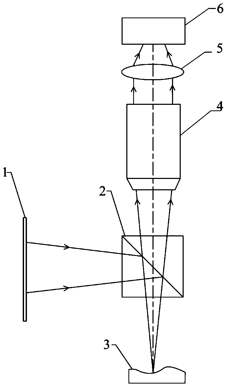
[0048] Such as figure 1Shown in an embodiment of the present invention, the optical deflection microscopic surface measurement device includes a projection screen 1, a beam splitting prism 2, an element to be measured 3, a microscopic objective lens 4, an imaging lens 5, a CCD detector 6 and a computer, Wherein, the component under test 3 is placed under the dichroic prism 2, the projection screen 1 is arranged on the left side of the dichroic prism 2 and the two are parallel, the microscopic objective lens 4, the imaging lens 5 and the CCD detectors 6 are sequentially arranged above the beam splitti...


PUM


Abstract

The invention discloses an optical deflection microscopic surface measuring method. The method comprises the following steps that a structural position parameter S of the optical deflection microscopic surface measuring device is measured and calibrated by adopting three-coordinate measuring equipment; phase distribution of a deformed fringe light signal is calculated according to the measured andcalibrated structural position parameter S, wherein the deformed fringe light signal comprises microscopic surface profile characteristic information of a to-be-measured element; actual light spot distribution corresponding to the microscopic surface of the to-be-measured element is acquired according to the phase distribution; and the actual light spot distribution is compared with preset ideallight spot distribution to obtain a microscopic surface profile of the to-be-measured element. Correspondingly, the invention further discloses an optical deflection microscopic surface measuring device. By means of the method and the device, the microscopic measurement technical scheme with the high precision, the low cost, the high spatial resolution and the high measurement speed is realized.

Description

technical field [0001] The invention relates to the field of measurement technology, in particular to an optical deflection microscopic surface measurement device and method. Background technique [0002] In recent years, with the development of micro-nano technology, the demand for the measurement of micro-deformation of components has gradually increased, and the requirements for measurement accuracy and speed have also continued to increase. In the prior art, the microscopic measurement of the reflective surface is usually achieved through technical solutions such as optical interferometer measurement method and scanning microscope measurement method. However, the optical interferometer measurement method has disadvantages such as small measurement dynamic range, susceptibility to environmental interference, and high detection cost. Scanning microscopy measurement methods, such as transmission electron microscopy (STEM), have extremely high horizontal and vertical resolu...

Claims


Application Information

Patent Timeline
Patent Type & Authority Applications(China)
IPC IPC(8): G01B11/25
CPCG01B11/254
Inventor 王道档吴振东孔明付翔宇许新科赵军刘维郭天太
Owner CHINA JILIANG UNIV
Why Eureka
Try Eureka