
TDD switching circuit and depletion type semiconductor amplification circuit

A switching circuit and amplifying circuit technology, which is applied in the field of TDD switching circuits and depletion-type semiconductor amplifying circuits, can solve the problems of high device cost and poor switching performance, and achieve the effect of improving performance and reducing costs

Pending Publication Date: 2020-02-07
苏州能讯微波集成电路有限公司
View PDF4 Cites 0 Cited by
  • Summary
  • Abstract
  • Description
  • Claims
  • Application Information

AI Technical Summary

Problems solved by technology

However, the cost of devices powered by negative voltage is high, and the switching performance is not as good as that of positive voltage devices.
[0006] Due to the above reasons, the negative voltage switch has become a technical short board for the TDD mode operation of GaN and other depletion semiconductor devices.
However, there is currently no effective solution to this problem

Method used


Image

  • TDD switching circuit and depletion type semiconductor amplification circuit
  • TDD switching circuit and depletion type semiconductor amplification circuit
  • TDD switching circuit and depletion type semiconductor amplification circuit

Examples


no. 1 example

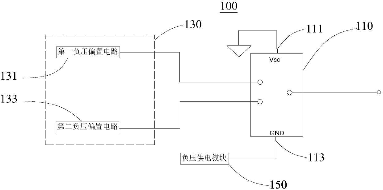
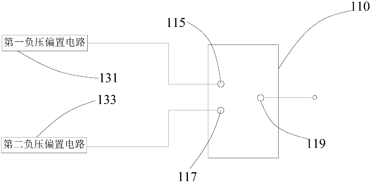
[0035] see in conjunction figure 1 and figure 2 , the present embodiment provides a TDD switch circuit 100, including a positive voltage switching device 110, a bias voltage module 130 and a negative voltage power supply module 150, the bias voltage module 130 is connected to the input end of the positive voltage switching device 110 for A first bias voltage signal and a second bias voltage signal are provided to the positive voltage switching device 110 . The output terminal of the positive voltage switching device 110 is used to connect to the back-end amplifier and selectively provide the first bias voltage signal or the second bias voltage signal to the back-end amplifier. Moreover, the positive voltage switching device 110 has a positive voltage power supply pin 111 and a ground pin 113 , and the negative voltage power supply module 150 is connected to the ground pin 113 for supplying power to the positive voltage switching device 110 . The positive voltage supply pin ...

no. 2 example

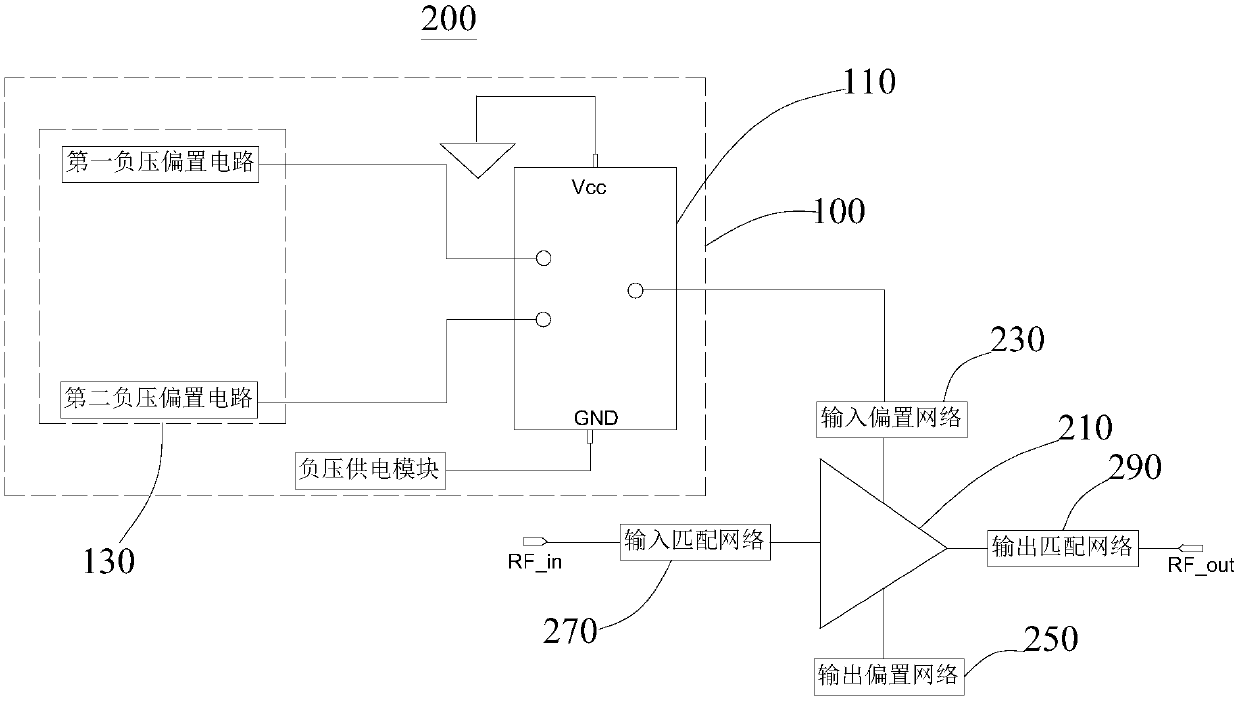
[0043] see in conjunction image 3 and Figure 4 , the present embodiment provides a depletion-type semiconductor amplifier circuit 200, including a back-end amplifier 210, a TDD switch circuit 100, an input bias network 230, an output bias network, an input matching network 270 and an output matching network 290, wherein The basic structure, principle and technical effects of the TDD switch circuit 100 are the same as those of the first embodiment. For a brief description, for parts not mentioned in this embodiment, reference may be made to the corresponding content in the first embodiment.

[0044] The TDD switch circuit 100 includes a positive voltage switching device 110, a bias voltage module 130 and a negative voltage power supply module 150, the bias voltage module 130 is connected to the input terminal of the positive voltage switching device 110, and is used to provide the positive voltage switching device 110 with a first The bias voltage signal and the second bias ...


PUM


Abstract

The invention provides a TDD switching circuit and a depletion type semiconductor amplification circuit. The TDD switching circuit comprises a positive voltage switching device, a bias voltage moduleand a negative voltage power supply module, the bias voltage module is connected with the input end of the positive voltage switching device, the output end of the positive-voltage switching device isused for being connected with a rear-end amplifier, the positive-voltage switching device is provided with a positive-voltage power supply pin and a grounding pin, the negative-voltage power supply module is connected with the grounding pin and used for supplying power to the positive-voltage switching device, and the positive-voltage power supply pin is connected to a reference ground so that the positive-voltage switching device can be in a positive-voltage power supply environment. In the TDD switching circuit, the power supply polarity of the positive-voltage power supply device is improved, so that the positive-voltage switching device can work in a negative-voltage power supply system without performance loss, the positive-voltage switching device replaces the original negative-voltage switching device, the cost is greatly reduced, and the performance of the switching device is improved.

Description

technical field [0001] The invention relates to the technical field of wireless communication, in particular to a TDD switch circuit and a depletion semiconductor amplifier circuit. Background technique [0002] In the fields of wireless communication, radar, data link, etc., RF power amplifier is an indispensable core link in related equipment. From the perspective of materials and processes, there are two types of RF power amplifier devices: enhanced devices and depletion devices; from the perspective of circuit architecture, the current common RF power amplifiers are Class A (Class A) power amplifiers, Class B (Class B) Class) power amplifier, Class AB (Class A and B) power amplifier, Class C power amplifier, feedforward power amplifier, envelope tracking (ET, EnvelopeTracking) power amplifier, envelope elimination and restoration (EER, Envelope Elimination and Restoration) power amplifier , Doherty (Doherty) power amplifier, etc. Among them, Class AB power amplifiers a...

Claims


Application Information

Patent Timeline
IPC IPC(8): H03K17/00
CPCH03K17/005H03K2217/0081
Inventor 万亮臧振刚王宇翔石尚杰
Owner 苏州能讯微波集成电路有限公司
Learn More