Method for testing resistivity of silicon carbide buffer layer

A test method and buffer layer technology, applied in semiconductor/solid-state device testing/measurement, circuits, electrical components, etc., can solve the problem of non-destructive, simple, fast and accurate silicon carbide high-concentration buffer layer resistivity, etc., Achieve fast and accurate results

Inactive Publication Date: 2020-02-14
HEBEI POSHING ELECTRONICS TECH
View PDF12 Cites 1 Cited by
  • Summary
  • Abstract
  • Description
  • Claims
  • Application Information

AI Technical Summary

Problems solved by technology

[0004] In view of this, an embodiment of the present invention provides a method for testing the resistivity of a silicon carbide buffer layer to solve the problem of non-destructive, simple, fast and accurate testing of the resistivity of a high-concentration silicon carbide buffer layer in the prior art. The problem

Method used


Image

  • Method for testing resistivity of silicon carbide buffer layer
  • Method for testing resistivity of silicon carbide buffer layer
  • Method for testing resistivity of silicon carbide buffer layer

Examples


Embodiment Construction

[0035] In the following description, specific details such as specific system structures and technologies are presented for the purpose of illustration rather than limitation, so as to thoroughly understand the embodiments of the present invention. It will be apparent, however, to one skilled in the art that the invention may be practiced in other embodiments without these specific details. In other instances, detailed descriptions of well-known systems, devices, circuits, and methods are omitted so as not to obscure the description of the present invention with unnecessary detail.

[0036] In order to illustrate the technical solutions of the present invention, specific examples are used below to illustrate.

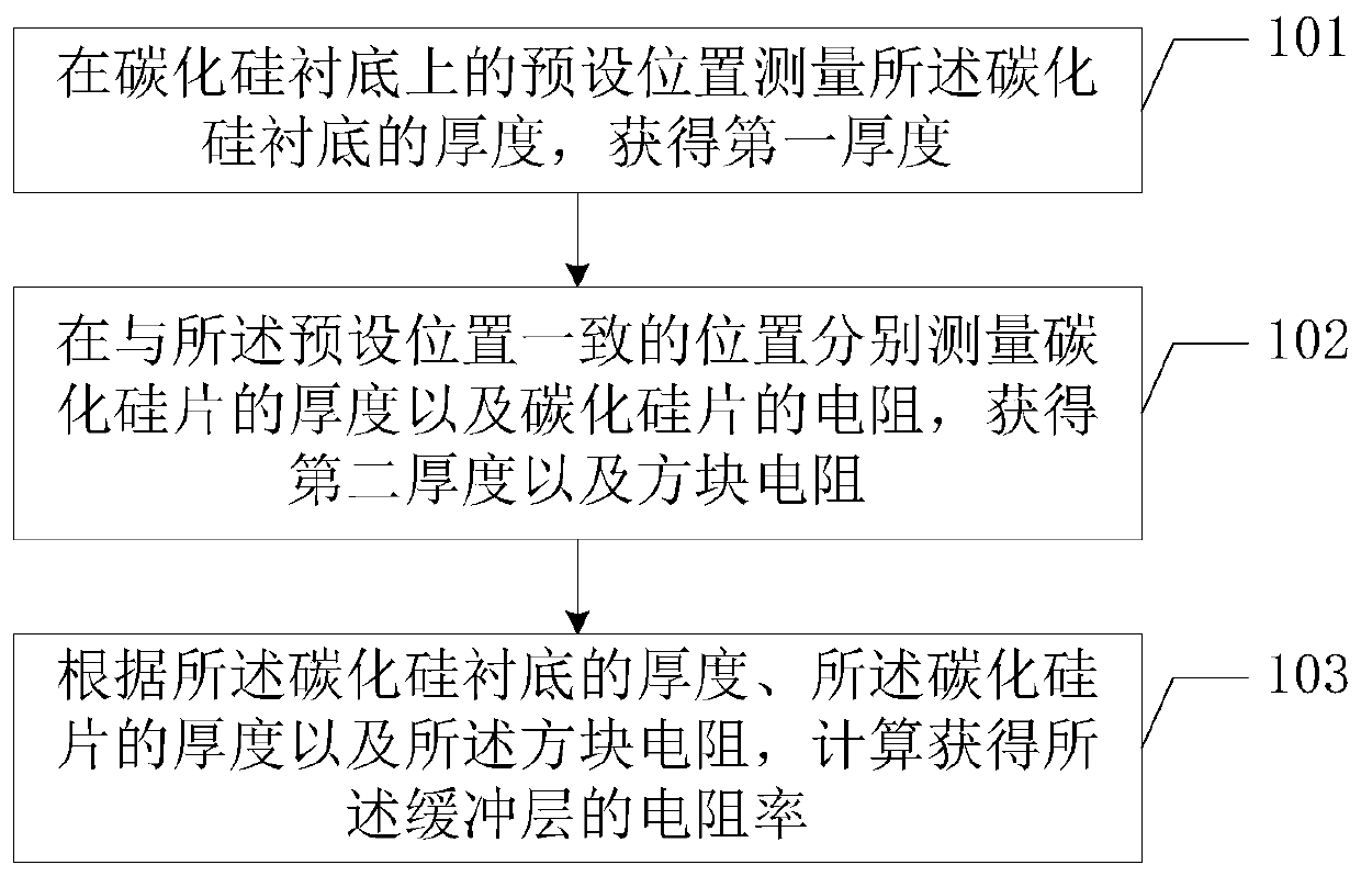
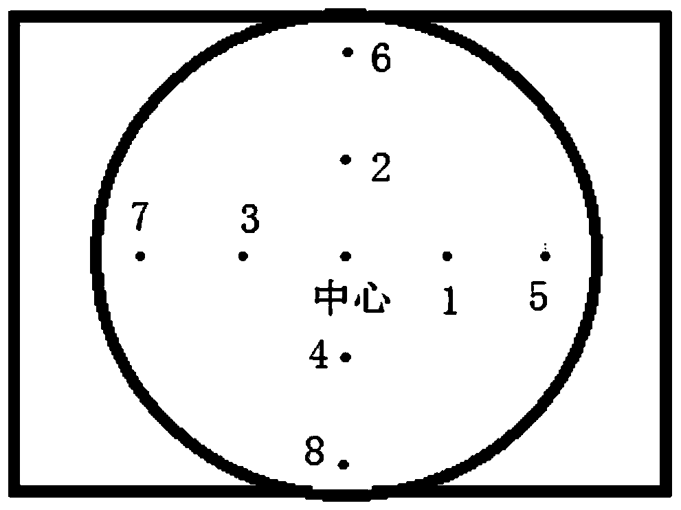
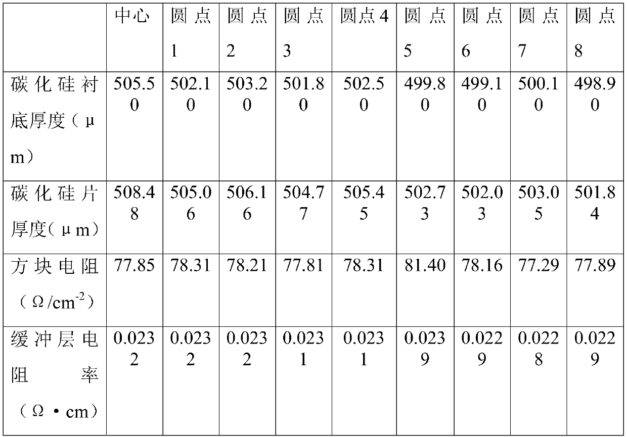
[0037] figure 1 The implementation flow diagram of a method for testing the resistivity of a silicon carbide buffer layer provided by an embodiment of the present invention is described in detail as follows.

[0038] Step 101, measuring the thickness of the silicon ca...


PUM

PropertyMeasurementUnit
Resistivityaaaaaaaaaa
Doping concentrationaaaaaaaaaa
Resistivityaaaaaaaaaa

Abstract

The invention belongs to the technical field of epitaxial growth of silicon carbide, and provides a method for testing resistivity of a silicon carbide buffer layer. The method comprises the followingsteps: measuring the thickness of a silicon carbide substrate at a preset position of the silicon carbide substrate so as to obtain a first thickness; separately measuring the thickness and the resistance of a silicon carbide wafer at a position identical with the preset position so as to obtain a second thickness and a square resistance, wherein the silicon carbide wafer is a sample obtained bygrowing a buffer layer on the silicon carbide substrate; and calculating the resistivity of the buffer layer according to the thickness of the silicon carbide substrate, and the thickness and the square resistance of the silicon carbide wafer. Thus, the resistivity of the buffer layer can be quickly and accurately obtained. The method for testing the resistivity of the silicon carbide buffer layerhas the advantages of free of damage, easiness, rapidness and high accuracy.

Description

technical field [0001] The invention belongs to the technical field of silicon carbide epitaxial growth, in particular to a method for testing the resistivity of a silicon carbide buffer layer. Background technique [0002] In order to reduce defects in the SiC epitaxial layer, a buffer layer with a high concentration is usually grown between the epitaxial drift layer and the SiC substrate. The grown high-concentration buffer layer can inhibit the propagation of silicon carbide substrate defects into the epitaxial layer and alleviate the lattice mismatch caused by the concentration difference between the substrate and the drift layer. Although the buffer layer greatly improves the quality of the epitaxial wafer, the buffer layer will increase the on-resistance of the device, thereby increasing the forward voltage of the device. Therefore, it is of great significance to control the parameters of the high-concentration buffer layer. [0003] At present, the silicon carbide e...

Claims


Application Information

Patent Timeline
IPC IPC(8): H01L21/02H01L21/66
CPCH01L21/02378H01L21/02447H01L22/14
Inventor 赵丽霞杨龙吴会旺
Owner HEBEI POSHING ELECTRONICS TECH
Why Eureka
Try Eureka