
PCB copper foil side cutting and board separating integrated equipment and PCB process line

A technology of splitting and cutting, which is applied in metal processing and other directions, can solve the problems of restricting production efficiency, high labor intensity, waste of resources, etc., and achieve the effects of reducing labor intensity, improving automation procedures, and reducing production costs

Active Publication Date: 2020-02-21
深圳恒鼎智能装备有限公司
View PDF6 Cites 8 Cited by
  • Summary
  • Abstract
  • Description
  • Claims
  • Application Information

AI Technical Summary

Problems solved by technology

[0003] 1. Waste of resources, increasing costs: Copper foil is a huge consumption and cost item in the PCB production process. Some PCB manufacturers do not cut and recycle the excess copper foil edges of PCB boards for production efficiency, which greatly wastes resources. and increased business costs
[0004] 2. Low work efficiency: Nowadays, when PCB boards are printed, it is common to manually cut the copper foil and divide the board, and the general cutting process line has a harsh environment and high labor intensity. Repeated manual work is prone to fatigue, and then It will restrict production efficiency, thereby affecting the benefits of the factory, and is not conducive to improving the market competitiveness of enterprises
[0005] 3. Affect the automation of the entire PCB industry, which is not conducive to the advancement of factory intelligence

Method used


Image

  • PCB copper foil side cutting and board separating integrated equipment and PCB process line
  • PCB copper foil side cutting and board separating integrated equipment and PCB process line
  • PCB copper foil side cutting and board separating integrated equipment and PCB process line

Examples


Embodiment Construction

[0041] The present invention will be described in detail below with reference to the drawings and specific embodiments.

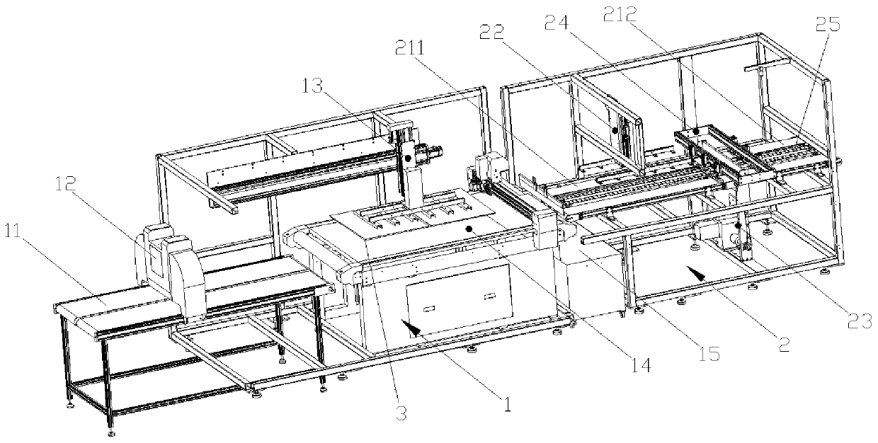
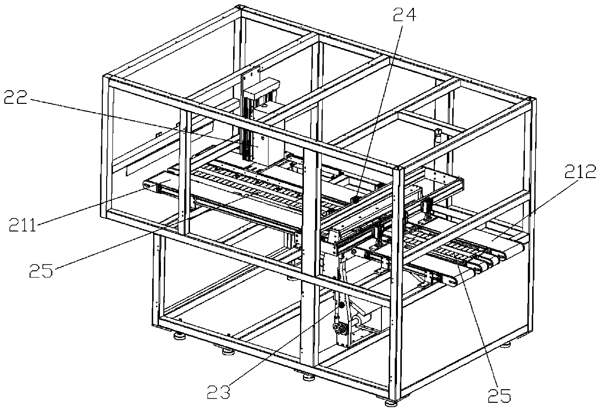
[0042] Such as figure 1 This embodiment provides an integrated device for cutting and separating PCB copper foil trims, including a PCB copper foil trim cutting and recycling device 1 and a PCB board automatic separation device 2. The PCB copper foil trim cutting and The recycling device is the front station, and the PCB board automatic dividing device is the rear station.

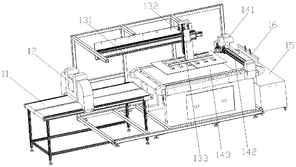
[0043] Such as figure 1 with figure 2 , The PCB copper foil trim cutting and recycling device includes: a feeding conveyor belt 11, a visual inspection device 12, a feeding manipulator, a cutting device, and a copper foil recovery box 15. The visual inspection device 12 is located on the feeding conveyor belt 11 Above, the cutting device is located on the side of the feeding conveyor belt 11, the feeding manipulator is located above the cutting device, and the copper foil recovery box 15 is...


PUM


Abstract

The invention discloses PCB copper foil side cutting and board separating integrated equipment and a PCB process line. The PCB copper foil side cutting and board separating integrated equipment comprises a PCB copper foil side cutting and recovery device and a PCB automatic separation device. The PCB copper foil side cutting and recovery device comprises a feeding conveying belt, a visual inspection device, a feeding mechanical arm, a cutting device and a copper foil recovery box. The PCB automatic separation device comprises a strip conveying belt, a position feedback system, an angle adjusting mechanical arm, a straw hopper board separation assembly, a board pressing assembly and a vacuum adsorption assembly. The PCB copper foil side cutting and recovery device is arranged to achieve PCBcopper foil side cutting, meanwhile, copper foil recovery is achieved, the PCB automatic separation device is used for carrying out automatic and precise board separation on PCBs, production efficiency is improved, the automatic procedure of a plant is improved, the labor intensive degree is reduced, production cost is reduced, and building of the intelligent plant is facilitated.

Description

Technical field [0001] The invention relates to the field of PCB production, in particular to an integrated equipment for cutting and dividing PCB copper foil edge materials and a PCB process line. Background technique [0002] At present, the disassembly process after PCB lamination does not have fully automated equipment. Most of them are manually operated to realize the trimming and recycling of excess copper foil, the splitting of multiple panels, and even some production process lines do not cut excess copper foil at all. On the other hand, its defects are as follows: [0003] 1. Waste of resources and increased cost: Copper foil is a huge expenditure item that consumes and spends a lot in the PCB production process. For production efficiency, some PCB manufacturers do not cut and recycle the excess copper foil edges of the PCB board, which greatly wastes resources. And increase business costs [0004] 2. Low work efficiency: At present, when PCB board is printed, it is genera...

Claims


Application Information

Patent Timeline
Patent Type & Authority Applications(China)
IPC IPC(8): B26D11/00B26D1/02B26D1/08B26D1/18B26D5/08B26D7/01B26D7/06B26D7/26B26D7/27
CPCB26D11/00B26D1/02B26D1/08B26D1/18B26D5/086B26D7/018B26D7/0625B26D7/2635B26D7/27B26D2011/005
Inventor 姚奇刘彩章王琦周杨彬
Owner 深圳恒鼎智能装备有限公司
Learn More