Manufacturing process of double-sided process sputtering film capacitive touch sensor

A double-sided process and capacitive touch technology, applied in the field of touch screens, can solve the problems of low process yield and process controllability, high vacuum requirements, large coating porosity, etc., to achieve process yield and process reliability The effect of high control degree, low vacuum requirement and small coating porosity

Pending Publication Date: 2020-02-21
WUXI MESH TECH CO LTD
View PDF4 Cites 0 Cited by
  • Summary
  • Abstract
  • Description
  • Claims
  • Application Information

AI Technical Summary

Problems solved by technology

[0004] The purpose of the present invention is to provide a manufacturing process of a double-sided process sputtering film capacitive touch sensor, which reasonably solves the uneven thickness of the ITO coating and metal coating in the manufacturing process of the prior art double-sided process capacitive touch sensor. Low adhesion, high vacuum requirements, large coating porosity, environmental pollution, low process yield and process controllability

Method used


Image

  • Manufacturing process of double-sided process sputtering film capacitive touch sensor
  • Manufacturing process of double-sided process sputtering film capacitive touch sensor
  • Manufacturing process of double-sided process sputtering film capacitive touch sensor

Examples


Embodiment Construction

[0021] Through the following description of the embodiments, it will be more helpful for the public to understand the present invention, but the specific embodiments given by the applicant cannot and should not be regarded as limitations on the technical solutions of the present invention, any components or technical features Changes to the definition and / or formal but not substantive changes to the overall structure should be regarded as the scope of protection defined by the technical solutions of the present invention.

[0022] Example:

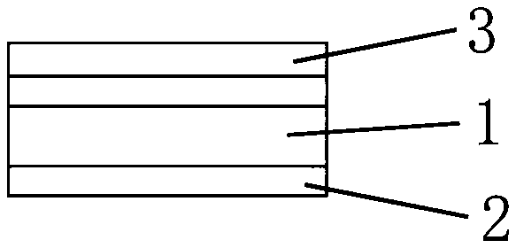
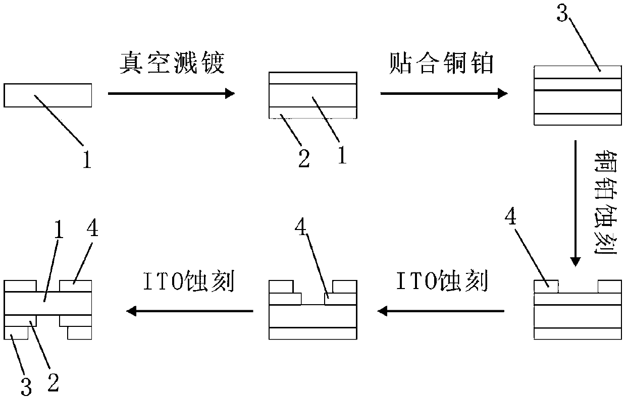
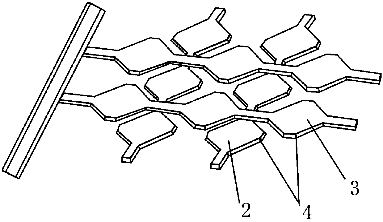
[0023] Such as Figure 1-3 The manufacturing process of a double-sided sputtering film capacitive touch sensor is shown, including a sputtering carrier plate 1, an ITO sputtering layer 2, a copper-platinum bonding layer 3, and a capacitive electrode 4. 1234

[0024] The manufacturing process of the double-sided process sputtering film capacitive touch sensor adopts that ITO sputtering layers 2 are respectively provided on both sides of th...


PUM


Abstract

The invention discloses a manufacturing process of a double-sided process sputtering film capacitive touch sensor. The manufacturing process comprises a sputtering carrier plate, an ITO sputtering layer, a copper-platinum laminating layer and a capacitor electrode. The process is characterized by further comprising the following steps: step 1, vacuum sputtering; step 2, copper-platinum laminating;step 3, double-sided etching; and step 4, setting of a sensor circuit. According to the invention, the ITO coating is arranged by vacuum sputtering, a copper-platinum metal layer structure is arranged on the ITO plating layer on one side in a rolling and fitting manner, and the copper-platinum layer and the ITO plating layer are etched by adopting a double-sided process etching process. The vacuum sputtering process is low in vacuum degree requirement, and the ITO sputtering layer is uniform, flat, thin, good in light transmission, high in plating layer adhesive force, small in plating layerporosity and high in process yield and process controllability. And the defects in the prior art are overcome.

Description

technical field [0001] The invention relates to the technical field of touch screens, in particular to a manufacturing process of a double-sided process sputtering film capacitive touch sensor. Background technique [0002] The production process of the double-sided process capacitive touch sensor in the prior art adopts evaporation to set the ITO coating, and then evaporates the structure of the metal coating on one side of the ITO coating, and then adopts the double-sided process etching process for the metal coating and the ITO coating. Etching results in uneven thickness of the ITO coating and metal coating, low adhesion of the coating, high vacuum requirements, large porosity of the coating, and low process yield and process controllability. [0003] The present invention adopts vacuum sputtering to set up the ITO coating layer, and then rolls and fits the copper-platinum metal layer structure on one side of the ITO coating layer, and then adopts a double-sided process ...

Claims


Application Information

Patent Timeline
Patent Type & Authority Applications(China)
IPC IPC(8): G06F3/044C23C14/08C23C14/34
CPCG06F3/044C23C14/34C23C14/086G06F2203/04103
Inventor 林行葛健国吕育仁范小荣朱育民庄胜智
Owner WUXI MESH TECH CO LTD
Why Eureka
Try Eureka