
High-Early-voltage lateral transistor structure and preparation method thereof

A lateral transistor, high-Early technology, applied in transistors, semiconductor/solid-state device manufacturing, circuits, etc., can solve the problems of transistor Early voltage reduction, lateral PNP base width reduction, low Early voltage, etc. Accuracy of doping concentration, good process compatibility, and the effect of improving the accuracy of line size control

Pending Publication Date: 2020-02-21
XIAN MICROELECTRONICS TECH INST
View PDF4 Cites 4 Cited by
  • Summary
  • Abstract
  • Description
  • Claims
  • Application Information

AI Technical Summary

Problems solved by technology

[0004] Compared with the NPN transistor, the Earley voltage of the traditional lateral PNP transistor is lower: when the CE voltage of the PNP transistor increases, the CB is in the reverse bias state, because the concentration of the P-type collector area of ​​the lateral PNP transistor is much higher than that of the N-type collector area, The CB junction space charge region mainly expands to the N-type base region, resulting in a rapid decrease in the width of the lateral PNP base region, and the significant widening effect of the base region leads to a decrease in the Earley voltage of the transistor.

Method used


Image

  • High-Early-voltage lateral transistor structure and preparation method thereof
  • High-Early-voltage lateral transistor structure and preparation method thereof
  • High-Early-voltage lateral transistor structure and preparation method thereof

Examples


Embodiment 1

[0052] The structure of the high Early voltage lateral PNP transistor of the present invention is as follows:

[0053] refer to Figure 3a with Figure 4 , the high Early voltage lateral PNP transistor includes an N-type epitaxial layer 1, and the upper part of the N-type epitaxial layer 1 is sequentially provided with a ring-shaped emitter region 61, a base region 5, and a collector contact lead-out region 62, wherein the collector region is provided with There is a collector contact lead-out area 62 .

[0054] Specifically, the lateral PNP transistor adopts a circular emitter region 61 with a diameter of 6 μm; a circular base region 5 with an inner diameter of 6 μm and an outer diameter of 30 μm; a 270° circular collector region 4 with an inner diameter of 30 μm and an outer diameter of 50 μm, and the collector region There is a 30°-360° circular collector contact lead-out area 62 with an inner diameter of 38 μm and an outer diameter of 42 μm; the P-type collector area 4 o...

Embodiment 2

[0065] The structure of the high Early voltage lateral PNP transistor of the present invention is as follows:

[0066] refer to Figure 3b with Figure 4 The high Early voltage lateral PNP transistor includes an N-type epitaxial layer 1, and the upper part of the N-type epitaxial layer 1 is sequentially provided with a ring-shaped emitter region 61, a base region 5, and a collector contact lead-out region 62, wherein the collector region is provided with There is a collector contact lead-out area 62 .

[0067] The lateral PNP transistor adopts a square emitter region with a side length of 4 μm; a square ring-shaped base region with an inner side length of 4 μm and an outer side length of 14 μm; a square ring-shaped collector region with an inner side length of 14 μm and an outer side length of 28 m. , A square annular collector contact lead-out area with an outer side length of 28 μm; the P-type collector area of ​​a lateral PNP transistor is doped with boron, and the impuri...

Embodiment 3

[0076] The emitter area of ​​the lateral PNP transistor is designed as a square or circular structure, and a multi-collector structure can be designed to obtain different ratios of collector current according to the surrounding range of different collector areas to the emitter area: refer to Figure 10 , such as a square emitter lateral PNP transistor design two collector regions: the first collector region 41 and the second collector region 42 where the first collector region 41 surrounds the three sides of the square emitter region, and the second collector region 42 surrounds One side of the square emitter region can obtain a collector current ratio of 3:1; for a lateral PNP transistor with a square emitter region, its multi-collector current is generally designed to be 1:1:1:1 (four collector regions , each collector area surrounds one side of the square emitter area), 2:1:1 (three collector areas, one collector area surrounds the two sides of the square emitter area, and t...


PUM


Abstract

The invention discloses a high-Early-voltage lateral transistor structure and a preparation method thereof. The lateral PNP transistor is formed by performing selective P-type impurity doping on an N-type epitaxial layer, that is, an emitter region of the PNP transistor is formed by a P-type doped region, a collector region of the PNP transistor is formed by a complete or partial annular P-type doped region outside the emitter region, and an N-type doped epitaxial layer is arranged between the two P-type doped regions to form a base region of the PNP transistor, so that a lateral P-N-P structure is formed, and the lateral PNP transistor is formed. Different from the traditional PNP transistor, the P-type collector region of the lateral PNP transistor with the novel structure is independently doped, the impurity concentration of the P-type collector region is lower than that of the N-type base region, when the CE voltage of the PNP transistor is increased, a CB junction space charge region is mainly expanded to the P-type collector region because the concentration of the P-type collector region of the lateral PNP transistor is lower than that of the N-type collector region, and thewidth change of the base region caused by the increase of the CE voltage is inhibited, so that a relatively high Early voltage is obtained.

Description

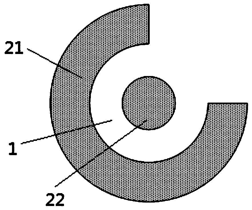
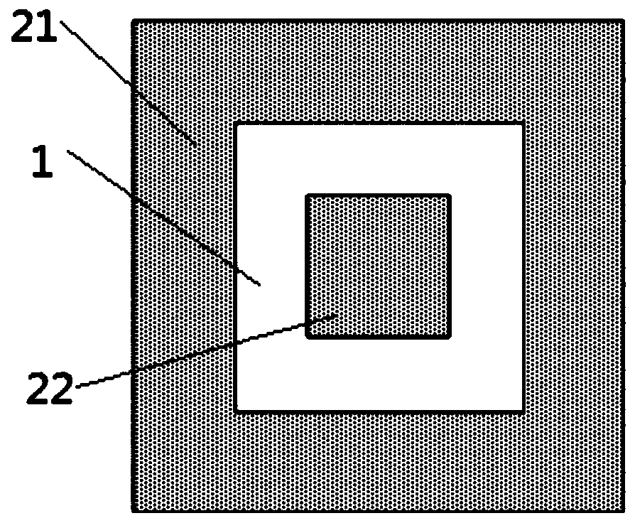
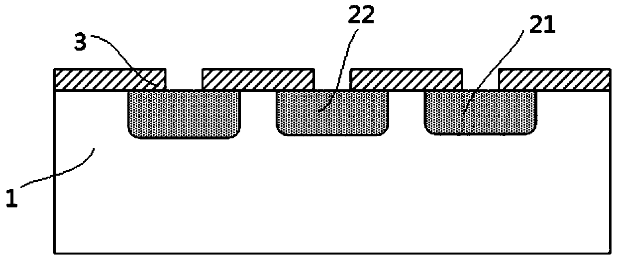
technical field [0001] The invention belongs to the technical field of transistors, and in particular relates to a high Early voltage lateral transistor structure and a preparation method thereof. Background technique [0002] The Early voltage is a parameter that characterizes the base widening effect of a bipolar transistor. For a bipolar transistor, the higher the Early voltage, the stronger its ability to suppress the base widening effect. [0003] refer to Figure 1a , Figure 1b with figure 2 , in the production of traditional bipolar integrated circuits, the P-type impurity doping of the collector region and emitter region of the lateral PNP transistor is carried out at the same level as the base region of the NPN transistor, that is, the P-type impurity doping is performed while forming the base region of the NPN transistor The P-type collector region and P-type emitter region of the lateral PNP transistor are formed, and the epitaxial layer is used as the N-type ...

Claims


Application Information

Patent Timeline
IPC IPC(8): H01L29/73H01L29/06H01L21/331
CPCH01L29/73H01L29/0603H01L29/0684H01L29/66234
Inventor 王清波薛东风赵杰薛智民孙有民杜欣荣温富刚卓青青
Owner XIAN MICROELECTRONICS TECH INST
Learn More