Reference voltage and voltage doubling circuit
A voltage doubling circuit and reference voltage technology, applied in the field of microelectronics, can solve the problems of increasing integrated chip area, increasing resistance, etc., and achieve the effect of small channel modulation effect, reducing area and improving stability
- Summary
- Abstract
- Description
- Claims
- Application Information
AI Technical Summary
Problems solved by technology
Method used
Image
Examples
Embodiment 1
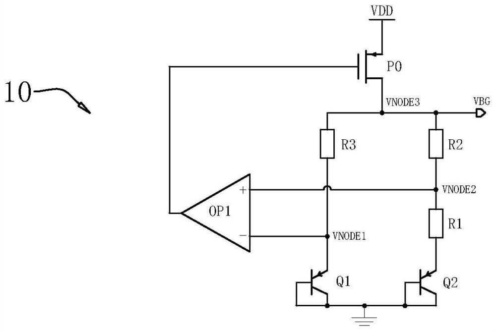
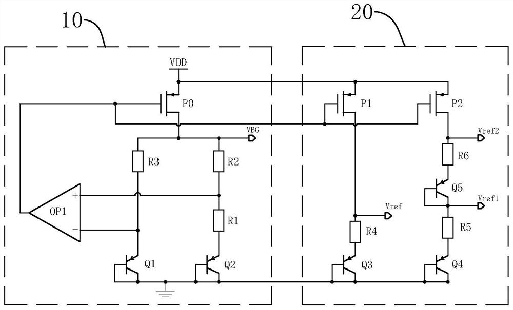
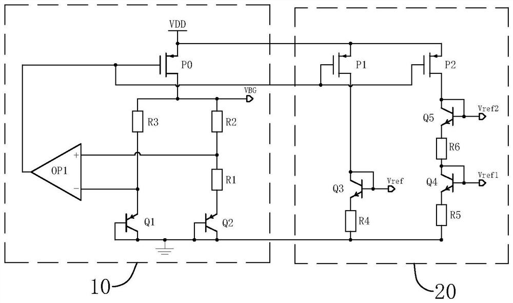
[0048] refer to Figure 6 The reference voltage and voltage doubler circuit includes a bandgap reference circuit 10 and a reference voltage doubler circuit 20, the bandgap reference circuit 10 is used to generate a bandgap reference voltage VBG.
[0049] The reference voltage doubler circuit 20 includes a MOS transistor N1, a current mirror unit 21 and a voltage doubler unit 22. The MOS transistor N1 adopts an N-type MOS transistor. The gate of the MOS transistor N1 is connected to the output end of the bandgap reference circuit 10, and the MOS transistor N1 The drain is connected to the current mirror unit 21, the source of the MOS transistor N1 is grounded, the current mirror unit 21 is connected to the power supply VDD, one end of the voltage doubler unit 22 is connected to the current mirror unit 21, and the other end of the voltage doubler unit 22 is grounded.
[0050] Wherein, the MOS transistor N1 adopts an isolated MOS transistor, which can better isolate the interfere...
Embodiment 2
[0062] refer to Figure 7 The difference between this embodiment and Embodiment 1 is that the output end of the bandgap reference circuit 10 is also connected to a filter unit 30. In this embodiment, the filter unit 30 includes a resistor R4 and a capacitor C, and one end of the resistor R4 is connected to The output end of the bandgap reference circuit 10 is connected, the other end of the resistor R4 is connected to the gate of the MOS transistor N1 and one end of the capacitor C, and the other end of the capacitor C is grounded.
[0063] The resistor R4 and the capacitor C1 form an RC filter network to filter the bandgap reference voltage signal VBG into a VBG_RC voltage signal, which can improve the stability of the reference voltage.
Embodiment 3
[0065] refer to Figure 8 The difference between this embodiment and Embodiment 2 is that the current mirror unit 21 also includes a MOS transistor P3, the MOS transistor P3 adopts a P-type MOS transistor, the source of the MOS transistor P3 is connected to the power supply VDD, and the gate of the MOS transistor P3 It is connected to the gate of the MOS transistor P1, and the drain of the MOS transistor P3 is connected to the reference voltage unit 40.
[0066] The reference voltage unit 40 includes a MOS transistor N5. The MOS transistor N5 is an N-type MOS transistor. The drain of the MOS transistor N5 is connected to the drain of the MOS transistor P3 and the gate of the MOS transistor N5. The source of the MOS transistor N5 is grounded. Wherein, the width of the MOS transistor N5 is 2um, and the length of the MOS transistor N5 is 20um. The voltage VGS generated on the MOS transistor N5 is equal to the bandgap reference voltage, therefore, the gate voltage of the MOS tran...
PUM
 Abstract
Description
Claims
Application Information


