Array substrate, manufacturing method thereof and display device

A technology of an array substrate and a manufacturing method, applied in the field of display devices, can solve the problems of reducing the transmittance of the pixel display area, reducing the display brightness, poor flexibility of the display device, etc., so as to improve the light transmittance and display brightness, and expand the application range. Effect

Pending Publication Date: 2020-02-25
BOE TECH GRP CO LTD
View PDF6 Cites 16 Cited by
  • Summary
  • Abstract
  • Description
  • Claims
  • Application Information

AI Technical Summary

Problems solved by technology

[0003] Among them, the traditional mirror display mostly uses a semi-transparent and semi-reflective film attached to the LCD (liquid crystal) display device to completely cover the pixel display area and the non-pixel display area to achieve a mirror display. Although the display back made by this method can achieve a mirror Display, but greatly reduces the transmittance of the pixel display area, and reduces the display brightness
Moreover, the flexibility of the display device is relatively poor, which reduces the scope of application of the display device

Method used


Image

  • Array substrate, manufacturing method thereof and display device
  • Array substrate, manufacturing method thereof and display device
  • Array substrate, manufacturing method thereof and display device

Examples


Embodiment Construction

[0042] Example embodiments will now be described more fully with reference to the accompanying drawings. Example embodiments may, however, be embodied in many forms and should not be construed as limited to the embodiments set forth herein; rather, these embodiments are provided so that this disclosure will be thorough and complete, and will fully convey the concept of example embodiments to those skilled in the art. The same reference numerals in the drawings denote the same or similar structures, and thus their detailed descriptions will be omitted.

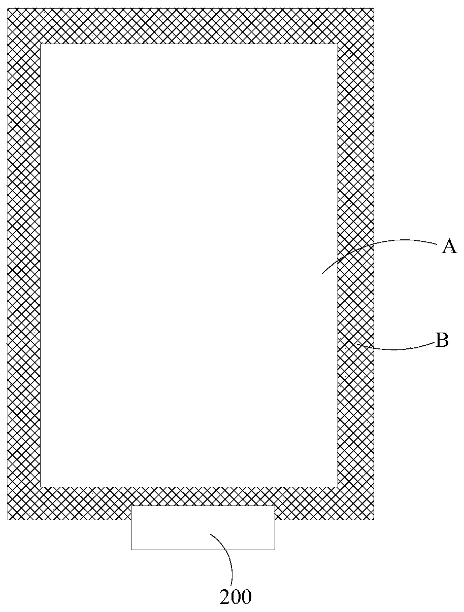
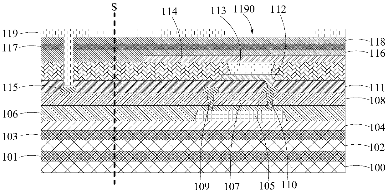
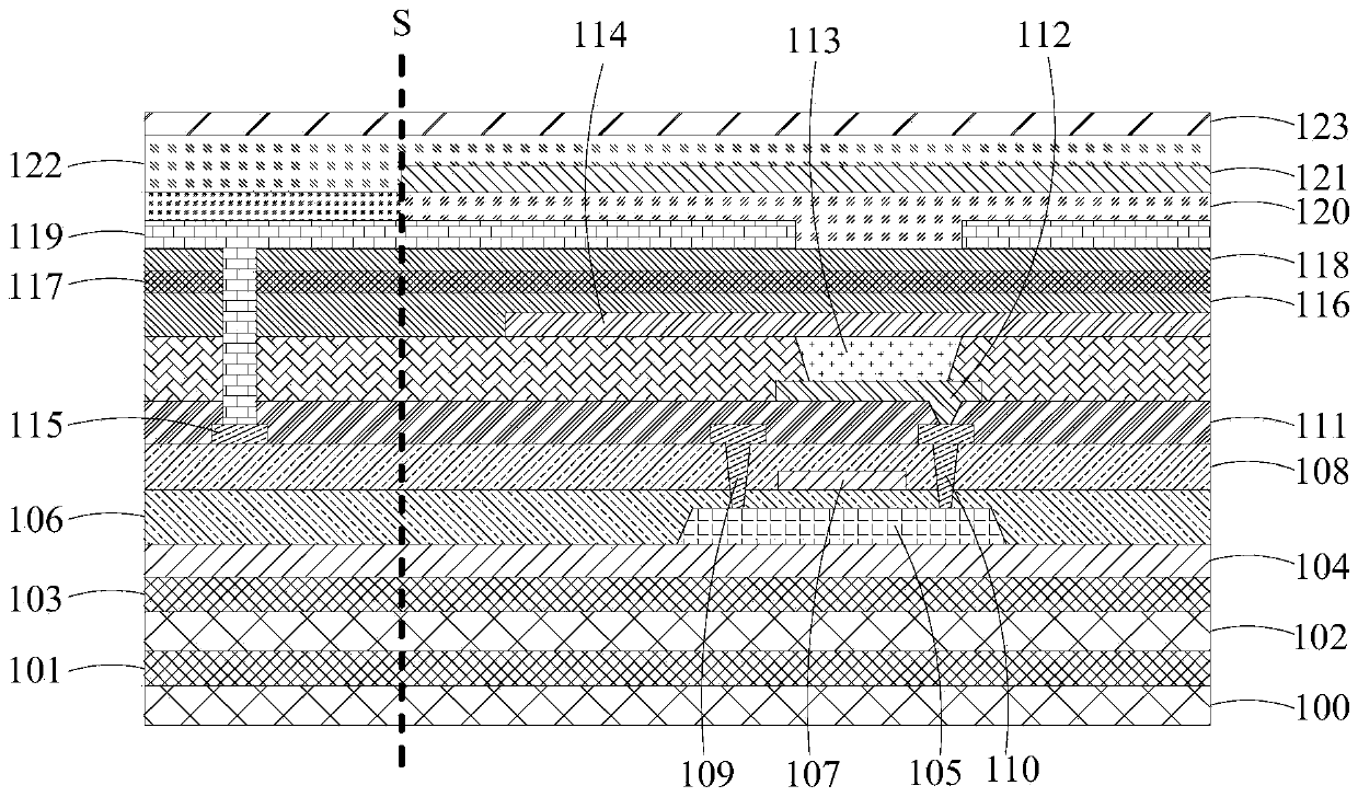
[0043] An embodiment of the present application provides an array substrate, such as figure 1 As shown, the array substrate has a display area A and a non-display area B located around the display area A. Specifically, the array substrate may include: a base substrate, a common ground signal line 115, a plurality of organic light emitting diodes, a packaging layer, and a metal reflective layer 119, wherein:

[0044] The base...


PUM


Abstract

The invention relates to an array substrate, a manufacturing method thereof and a display device. The array substrate is provided with a display area and a non-display area located on the periphery ofthe display area. The array substrate comprises a substrate, a common grounding signal line, multiple organic light-emitting diodes, a packaging layer and a metal reflecting layer, wherein the commongrounding signal line is formed on the substrate and located in the non-display area; the organic light-emitting diodes are formed on the substrate and located in the display area, and cathodes of the organic light-emitting diodes are electrically connected with the common grounding signal line; the packaging layer is formed on the substrate and covers the organic light emitting diode; the metalreflecting layer is formed on the packaging layer and located in the display area, the metal reflecting layer is provided with a plurality of light holes, and each light hole corresponds to one organic light emitting diode; the orthographic projection of the light hole on the substrate covers the orthographic projection of the organic light-emitting layer of the organic light-emitting diode on thesubstrate; and the metal reflecting layer is electrically connected with the common grounding signal line. According to the array substrate and the display device, the light transmittance and the display brightness are improved while mirror surface display is realized.

Description

technical field [0001] The present invention relates to the field of display technology, in particular, to an array substrate, a manufacturing method of the array substrate, and a display device. Background technique [0002] At present, the market demand for products that combine mirrors and displays is becoming more and more widespread. They are not only applied to home furnishing, shopping malls, advertising, beauty and cosmetics, but also to vehicle rearview mirrors and other application scenarios. [0003] Among them, the traditional mirror display mostly uses a semi-transparent and semi-reflective film attached to the LCD (liquid crystal) display device to completely cover the pixel display area and the non-pixel display area to achieve mirror display. Although the display back made by this method can realize mirror display Display, but the transmittance of the pixel display area is greatly reduced, and the display brightness is reduced. Moreover, the flexibility of t...

Claims


Application Information

Patent Timeline
Patent Type & Authority Applications(China)
IPC IPC(8): H01L27/32
CPCH10K59/123H10K59/1213H10K59/1315H10K59/12
Inventor 盖人荣刘利宾
Owner BOE TECH GRP CO LTD
Why Eureka
Try Eureka