Processing method of stack-bonded wafer

A processing method and wafer technology, which is applied in the direction of electrical components, semiconductor/solid-state device manufacturing, circuits, etc., can solve problems such as yield loss, and achieve the effects of avoiding yield loss, avoiding wafer edge reduction, and stabilizing the cutting process

Inactive Publication Date: 2020-02-28
ICLEAGUE TECH CO LTD +1
View PDF15 Cites 4 Cited by
  • Summary
  • Abstract
  • Description
  • Claims
  • Application Information

AI Technical Summary

Problems solved by technology

[0004] When there is a stack of multi-layer wafers, the abnormal part of the edge must be removed every time the wafer is bonded and stacked and thinned. Therefore, after multi-layer wafer stacking, the part of the edge cut will be considerable, resulting in a loss of yield

Method used


Image

  • Processing method of stack-bonded wafer
  • Processing method of stack-bonded wafer
  • Processing method of stack-bonded wafer

Examples


Embodiment Construction

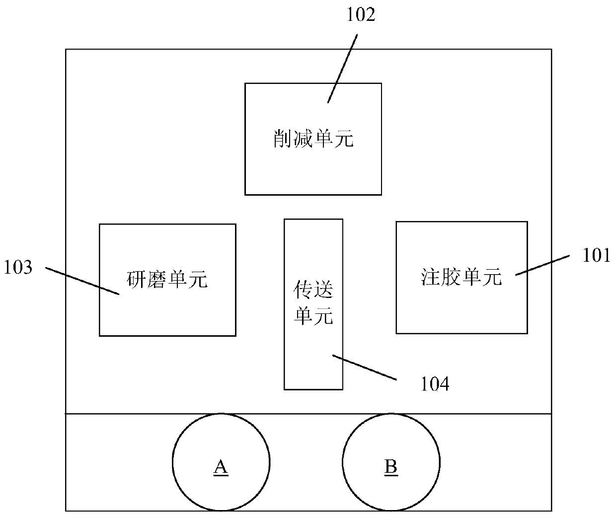
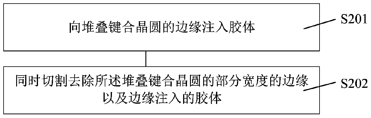
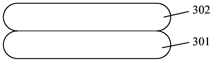
[0023] As mentioned in the background art, when conventional multi-layer wafers are stacked, the edge cuts will be considerable, resulting in a loss of yield.

[0024] The study found that when stacking multi-layer wafers, after each wafer stacking, the corresponding wafers must be thinned. After the thinning operation, an edge reduction process is required, so When stacking multi-layer wafers, multiple thinning operations and multiple trimming processes are required. Therefore, when multi-layer wafers are stacked, the edge trimming will be considerable, resulting in a loss of yield. And because defects such as cracks may spread to the center of the wafer every time the thinning is performed, the width to be cut will be wider when the edge is cut next time, which further increases the amount of cuts on the edge of the stacked wafer and further causes good rate loss. And the process has been cut many times, which reduces the production efficiency.

[0025] To this end, the pr...


PUM


Abstract

The invention provides a processing method of a stack-bonded wafer. The processing method comprises the steps: injecting colloid into the edge of stack-bonded wafer; and cutting and removing the edgeof partial width of the stack-bonded wafer and the colloid injected at the edge. When the stack-bonded wafer processing machine processes multi-layer stacked bonded wafers, after each time of glue injection and grinding of the two bonded wafers, no glue removal and cutting (cutting) steps are required. After the multi-layer stacked bonded wafers are formed, the edge of the partial width of the stack-bonded wafer and the colloid injected into the edge can be simultaneously cut and removed by performing one step of cutting process by the cutting unit so that excessive wafer edge cutting caused by multiple times of cutting in the manufacturing process of the multi-layer stacked wafers can be avoided and further excessive yield loss can be avoided.

Description

technical field [0001] The invention relates to the field of semiconductors, in particular to a method for processing stacked and bonded wafers. Background technique [0002] With the advent of the stacked chip era, edge trimming (edge ​​trimming) technology is also increasingly important. Wafer edge reduction is to use a dicing blade to cut a part of the edge of the stacked wafer, and remove the abnormal part of the stacked wafer. [0003] An existing cutting process includes: providing a first wafer and a second wafer; bonding the first wafer and the second wafer to form a stacked bonded wafer; The two wafers are thinned; after the thinning, the edges of part of the width of the stacked and bonded wafers are removed, so as to remove the edge abnormalities of the stacked and bonded wafers. [0004] When there is a stack of multi-layer wafers, it is necessary to remove the abnormal part of the edge every time the wafer is bonded and stacked and thinned. Therefore, after mu...

Claims


Application Information

Patent Timeline
Patent Type & Authority Applications(China)
IPC IPC(8): H01L21/02H01L21/18
CPCH01L21/02021H01L21/0201H01L21/185
Inventor 余兴蒋维楠
Owner ICLEAGUE TECH CO LTD
Why Eureka
Try Eureka