Flexible thin film substrate, preparation method thereof, display panel and display device

A flexible film and substrate technology, which is applied in semiconductor/solid-state device manufacturing, electrical components, electric solid-state devices, etc. Regional stress concentration and other issues can be avoided to avoid film fracture, avoid internal stress increase, and improve bending performance

Inactive Publication Date: 2020-02-28
WUHAN CHINA STAR OPTOELECTRONICS SEMICON DISPLAY TECH CO LTD
View PDF6 Cites 4 Cited by
  • Summary
  • Abstract
  • Description
  • Claims
  • Application Information

AI Technical Summary

Problems solved by technology

[0005] An embodiment of the present invention provides a flexible thin film substrate, which is used to solve the problem of the flexible substrate in the prior art. After the thin film transistor is prepared on the flexible substrate, the stress neutral line in the bending area and the metal wiring layer are not uniform, resulting in Stress concentration is prone to occur in the bending area, and the technical problems of bending and fracture of the metal wiring layer

Method used


Image

  • Flexible thin film substrate, preparation method thereof, display panel and display device
  • Flexible thin film substrate, preparation method thereof, display panel and display device
  • Flexible thin film substrate, preparation method thereof, display panel and display device

Examples


Embodiment Construction

[0033] The following will clearly and completely describe the technical solutions in the embodiments of the present invention with reference to the accompanying drawings in the embodiments of the present invention. Obviously, the described embodiments are only some, not all, embodiments of the present invention. Based on the embodiments of the present invention, all other embodiments obtained by those skilled in the art without making creative efforts belong to the protection scope of the present invention.

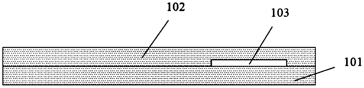
[0034] In the flexible substrate of the prior art, after the thin film transistor is prepared on the flexible substrate, the stress neutral line in the bending area is not consistent with the metal wiring layer, which leads to stress concentration in the bending area and the metal wiring layer The problem of bending fracture, this embodiment can solve this defect.

[0035] Such as figure 1 As shown, the basic structural diagram of the flexible film substrate provided by ...


PUM

PropertyMeasurementUnit
thicknessaaaaaaaaaa
widthaaaaaaaaaa
thicknessaaaaaaaaaa

Abstract

The present invention provides a flexible thin film substrate including a flexible substrate. The flexible substrate including a first substrate layer and a second substrate layer that are stacked. The second substrate layer is disposed over the first substrate layer. The bending region of the second substrate layer is provided with at least one groove. In the present invention, the groove is formed in the bending region of the flexible substrate to reduce the thickness of the substrate in the bending region so that the stress neutral line in the bending region approaches a metal wiring layer,thereby improving the bending resistance of the flexible thin film substrate, and avoiding problems such as an increase internal stress and film breakage in the bending region. The flexible thin filmsubstrate structure of the present invention includes at least two stacked substrate layers to meet the requirements for high flexibility, heat resistance, high water and oxygen resistance.

Description

technical field [0001] The invention relates to the field of display technology, in particular to a flexible film substrate and a preparation method thereof, a display panel, and a display device. Background technique [0002] With the rapid development of display technology, the field of display panels is developing towards lighter, thinner, softer, and more transparent. Traditional glass substrates are difficult to meet the requirements of future flexible display technology due to their own hard and brittle characteristics. The polymer film substrate has the characteristics of light weight, flexibility, and excellent comprehensive performance, which can well meet the flexibility requirements of future flexible display technology. Therefore, flexible polymer substrate materials are the materials of choice for future flexible display technologies. [0003] At present, the most promising polymer material for flexible substrates is polyimide, which has excellent heat resistan...

Claims


Application Information

Patent Timeline
Patent Type & Authority Applications(China)
IPC IPC(8): H01L27/12H01L21/77
CPCH01L27/1218H01L27/1244H01L27/1262
Inventor 柯霖波
Owner WUHAN CHINA STAR OPTOELECTRONICS SEMICON DISPLAY TECH CO LTD
Why Eureka
Try Eureka